
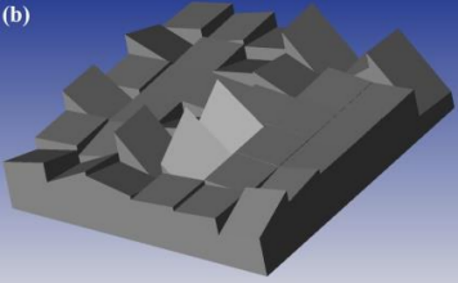
Influence of Parameters in the Design of a Faceted Structure for Incoherent Beam Shaping
Authors: Lihong Liu, Thierry Engel, Huwen Ding et al.Institution:Institute of Microelectronics, Chinese Academy of Sciences, Beijing
Keywords:Incoherent beam shaping;micro lens array;custom optimization
doi:10.33079/jomm.21040401
Abstract:
A reflective faceted structure is proposed to reshaping an incoherent light beam into two focalized spots. To obtain the desired irradiance distribution on a detector, custom optimization function ...
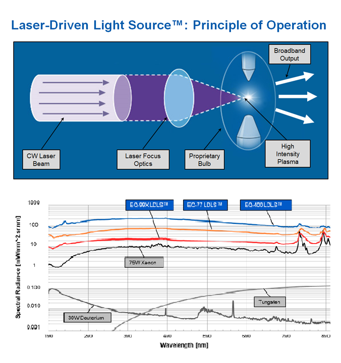
Laser-Driven Light Sources for Nanometrology Applications
Authors: Huiling Zhu, Paul BlackborowInstitution:Energetiq Technology, Inc, ., 7, Constitution Way, Woburn
Keywords:laser-driven;brightness;broadband;deep-UV;metrology;LDLS
doi:10.33079/jomm.19020104
Abstract:
Laser-driven light sources (LDLS) have ultrahigh-brightness and broad wavelength range. They are ideal radiation sources for optical metrology tools for advanced process control in semiconductor ma...
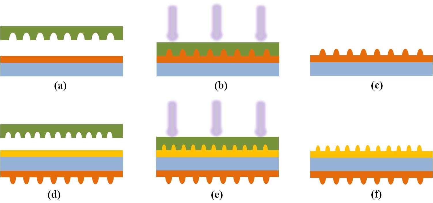
Preparation of Double-sided Nanostructure Based on Soft-nanoimprinting Lithography
Authors: Man Zhang, Qiling Deng, Hui Pang et al.Institution:Institute of Optics and Electronics, Chinese Academy of Sciences
Keywords:Double-sided nanostructure, elastic substrate, soft-nanoimprinting lithography, metal layer.
doi:10.33079/jomm.18010201
Abstract:
Double-sided nanostructure has more excellent properties in high efficiency, high yield, and high capability devices, which becomes the attention spots in nanofabrication technology. We proposed a ...
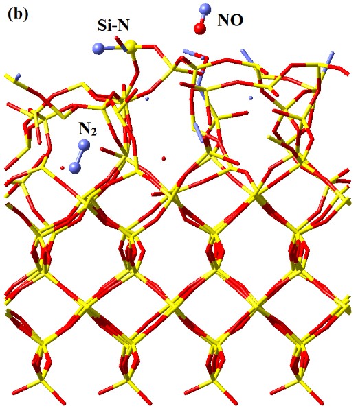
Nitridation-Etch of Silicon Oxide in Fluorocarbon/Nitrogen Plasma: A Computational Study
Authors: Du Zhang, Yu-Hao Tsai, Hojin Kim et al.Institution:TEL Technology Center, America, LLC, 255, Fuller Road, Suite, 214, Albany
Keywords:3D-NAND;oxide;nitride;oxynitride;plasma etch;molecular dynamics;quantum chemistry
doi:10.33079/jomm.19020103
Abstract:
The continually increasing number of silicon oxide (SiO2) and nitride (Si3N4) layers in 3D-NAND offers both motivations and challenges for developing all-in-one pla...
Improvement of Environment Stability of an i-Line Chemically Amplified Photoresist
Authors: Haibo Li, Qian Yang, Jia Sun et al.Keywords:Chemical amplification;thick film;i-Line;environment stability;Poly (p-hydroxyl styrene);PAB;PEB
doi:10.33079/jomm.21040201
Abstract:
An i-Line chemically amplified (ICA) thick film positive resist is reported in this paper. The impact of process conditions on photoresist performance was investigated. Pre-apply bake temperature a...
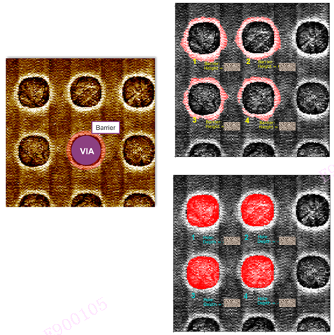
Novel Pattern-Centric Solution for XtackingTM AFM Metrology
Authors: Sicong Wang, Jian Mi, Abhishek Vikram et al.Institution:Yangtze Memory Technologies Co, ., Ltd, Wuhan
Keywords:VIA;Dishing;AFM;Image;Metrology;3D NAND
doi:10.33079/jomm.19020403
Abstract:
3D NAND (three-dimensional NAND type) has rapidly become the standard technology for enterprise flash memories, and is also gaining widespread use in other applications. Continued manufacturing pro...
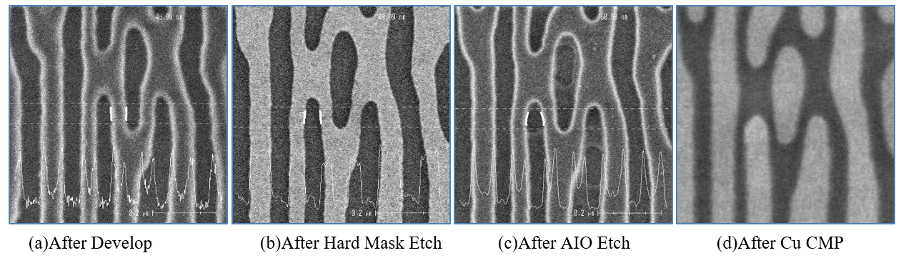
Patterning Defect Study for Process Integration Engineering Using Pattern Fidelity Monitoring with Review SEM Images
Authors: Yu Zhang, Abhishek Vikram, Ming Tian et al.Institution:Shanghai Huali Microelectronics Corp, ., Pudong District, Shanghai
Keywords:Die-to-database Pattern Monitor;After Develop Inspection (ADI);After Etch Inspection (AEI);SEM Review;CDSEM;pattern centric;pattern monitor
doi:10.33079/jomm.19020203
Abstract:
Normally the optical wafer inspection tools are used for advanced process control in high volume manufacturing of semiconductor devices. The SEM Review is done for limited sample of inspection defe...
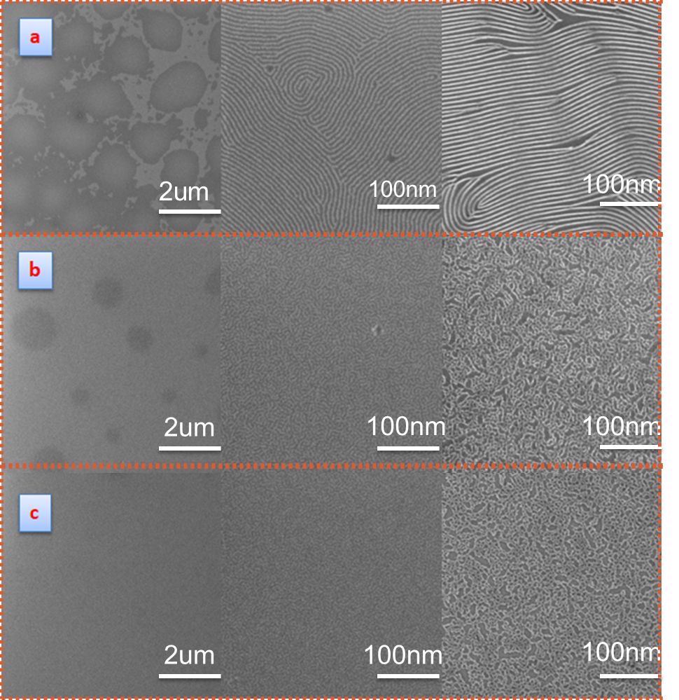
Self-assembly of Blended PS-b-P2VP Block Copolymers
Authors: Baolin Zhang, Yu Chen, Shisheng XiongInstitution:School of Information Science and Technology, Fudan University, Shanghai
Keywords:Micro-phase;blending;lamellar pattern;solvent annealing;sequential infiltration synthesis
doi:10.33079/jomm.19020404
Abstract:
Directed Self-Assembly (DSA) of block copolymers (BCPs) is a promising technique for sub-10 nm nanofabrication, which is highly compatible with conventional lithography. DSA relies on the microphas...
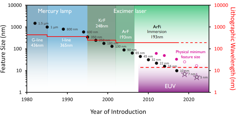
EUV Lithography: State-of-the-Art Review
Authors: Nan Fu, Yanxiang Liu, Xiaolong Ma et al.Institution:HiSilicon Technologies Co, ., Ltd, Shanghai
Keywords:EUV lithography;EUV review;mask 3D;line edge roughness;EUV light source
doi:10.33079/jomm.19020202
Abstract:
Although several years delayed than its initial plan, extreme UV lithography (EUVL) with 13.5nm wavelength has been finally implemented into high volume manufacture (HVM) of mainstream semiconducto...
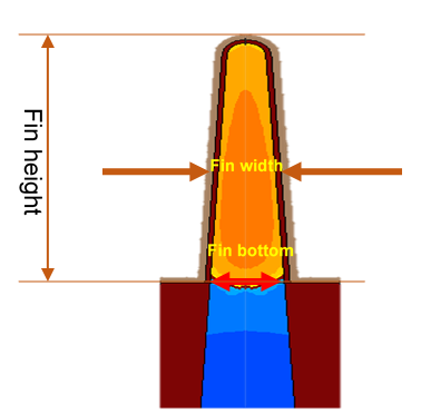
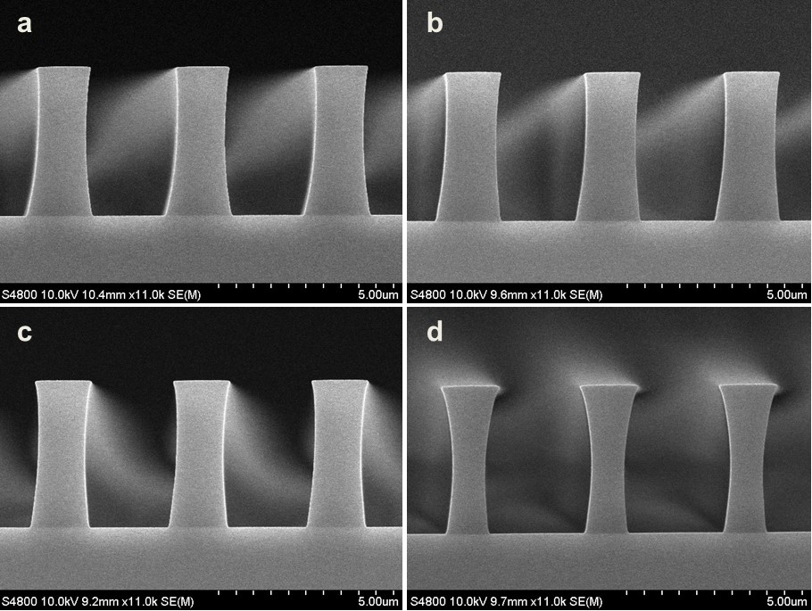
The Effect of Fin Structure in 5 nm FinFET Technology
Authors: Enming Shang, Yu Ding, Wenqiao Chen et al.Institution:Shanghai IC R, &, D Center, Shanghai
Keywords:5 nm;FinFET;fin profile;semiconductor
doi:10.33079/jomm.19020405
Abstract:
In 5 nm technology node, FinFET device performance is sensitive to the dimension of the device structure such as the fin profile. In this work, we simulate the influence of fin height and fin width...