Research Article Archive Versions 2 Vol 2 (4) : 19020403 2019
Download
Novel Pattern-Centric Solution for XtackingTM AFM Metrology
: 2019 - 11 - 06
: 2019 - 12 - 25
1975 35 0
Abstract & Keywords
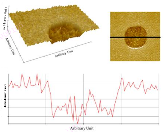
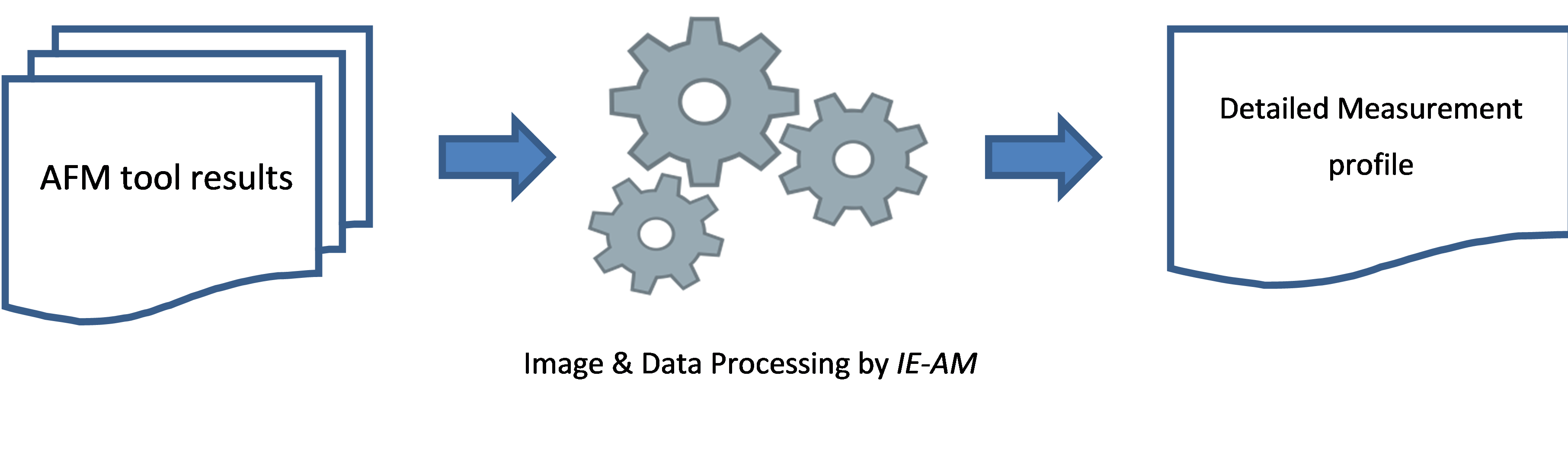
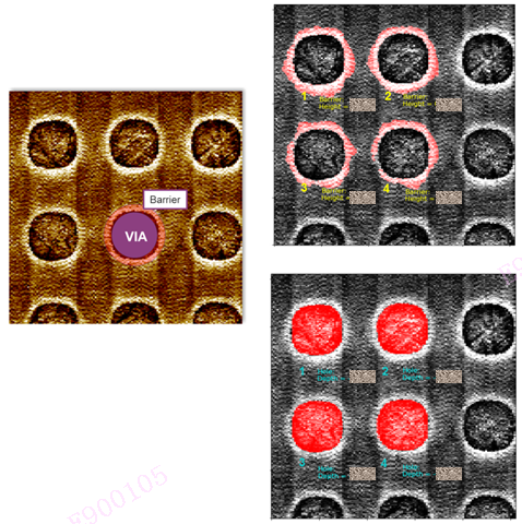
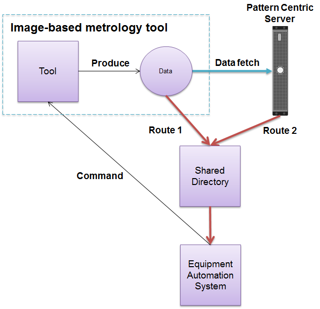
Abstract: 3D NAND (three-dimensional NAND type) has rapidly become the standard technology for enterprise flash memories, and is also gaining widespread use in other applications. Continued manufacturing process improvements are essential in delivering memory devices with higher I/O performance, higher bit density, and at lower cost. Current 3D NAND technology involves process steps that form array and peripheral CMOS (Complementary Metal-Oxide-Semiconductor) regions side-by-side, resulting in waste of silicon real estate and film stress compromises, and limits the paths of making advanced 3D NAND devices. An innovative architecture was invented to overcome these challenges by connecting two wafers electrically through metal VIAs (Vertical Interconnect Access) [1]. Highly accurate and efficient metrology is required to monitor VIA interface due to increased process complexity and precision requirements. With the advanced processing of AFM (Atomic Force Microscopy) images, highly accurate and precise measurements have been achieved. An inline pattern-centric metrology solution that is designed for high volume mass production of high-performance 3D NAND is presented in this paper.
Keywords: VIA; Dishing; AFM; Image; Metrology; 3D NAND
1.   Introduction
The VIA interface topography, which normally resembles a dishing shape to ensure connection between wafers, is one of the most important factors in determining the quality of wafer interconnection. A suitable monitoring scheme for VIA dishing is necessary to avoid structural and reliability issues such as interconnection open, metal void, metal diffusion, etc. The industry has developed several methods in the product development flow to proactively identify these hotspots, also known as weak points [2-4]. Despite all such design verification methods, we must still employ aggressive metrology methods to detect any deformation during fabrication [5, 6]. The depth of VIA dishing could be very small in order to meet the requirements of good interconnection. Thus, ultra-precise measurement in vertical direction is needed. AFM appears to be the only reliable metrology method for this purpose. Yet it still poses two primary metrology challenges. Firstly, the shallow depth makes it difficult for capturing the edges of these VIA features on wafer. Frequent capturing failures happen when measuring VIA dishing because of the small average depth. Also, partial capturing and unwanted pixels exacerbate the difficulty in accurate measurement. Secondly, the dishing depth varies depending on metal volume and density distribution that is caused by chip layout, which leads to potential weak points. So to monitor these weak points, a metrology method with advanced pattern recognition is required that can handle the complex VIA arrangement. In order to address these challenges, we have utilized a complementary approach. The measurement results obtained from the AFM tool undergo an advanced Image and Data Processing (IDP) application of IE-AM (Image Explorer for Advanced Metrology) while maintaining the original measurement accuracy and precision of the AFM tool. Several real case scenarios have been successfully tested with this integrated approach. Further in this paper we describe the requirement for such an IDP approach for improving the VIA dishing metrology and then explain the methodology with real case results. In the last section we explain the integration of IE-AM solution with the existing fabrication infrastructure to achieve full automation.
2.   VIA Topography Requirement for Wafer Connection
Traditional approach to connecting wafers is by using VIA, but metal in the VIA exhibits higher coefficient of thermal expansion (CTE) compared to silicon and dielectrics in the wafer, and this induces large stresses in both the metal plugs and the surrounding silicon. The large thermo-mechanical stress can be mitigated by proper CMP process. In a study of a CMP process resulting in VIA shape that is slightly protruding on the top wafer and slightly dishing in the bottom wafer, thus allowing for necessary wafer to wafer overlay bonding tolerance, better overall resistivity and yield were achieved[7].
Prior to wafer connection, the dishing and protruding specifications are set based on the potential defects. Risk of open circuit is minor considering the expansion, but for dishing condition, metal-metal interface voids and seams have been observed [8-10]. On the other hand, metal diffusion at interface will cause more severe issues to electrical function and reliability. Therefore, dishing depth and/or protruding height should be small enough to meet wafer connection requirement. VIA shape monitor thus needs to be built by inline AFM after the completion of CMP, and before wafer bonding process.
A fundamental challenge of AFM metrology is the compromise between throughput and resolution. A typical inline bottom wafer AFM metrology setup is done at 1 Hz scanning rate with 500 x 500 pixels. In this paper we discuss mainly the dishing wafer condition. To measure the average dishing depth, VIA edge should be recognized as the VIA area and dielectric is isolated at the edge. The image of metal VIA and dishing profile are schematically shown in Figure1. Smaller depth could lead to insufficient contrast at the VIA edge, randomly causing pattern recognition misalignment and measurement failure on the AFM tool. Therefore, an additional image processing method is needed for AFM image analysis.


Figure 1.   Typical AFM image of wafer VIA bottom; dishing is achieved by CMP process.
The Cu CMP process contains three polishing steps including Cu bulk, Cu clear and barrier CMP. Each individual polishing step is highly selective to the material; the primary factor affecting the dishing depth is metal volume. Variation of metal volume leads to non-uniform distribution of dishing profile, thus causing creation of weak points throughout the whole chip. In order to deal with complex patterns throughout the chip there is a need for a pattern-centric solution for AFM data analysis. Indeed, better image processing is desired for automatic AFM measurement of advanced 3D-NAND development and production.
3.   Methodology
The new approach is complementary in nature and does not disrupt the existing metrology flow. The measurement data obtained from the AFM tool is fed into an Image and Data Processing (IDP) application of IE-AM, as shown in Figure 2, which analyzes each feature in individual images to generate a consolidated metrology profile. The result obtained directly from the AFM tool consists of the target image with the associated measurement files. The IDP application focuses on the feature of interest in each image and extracts the contour pattern.


Figure 2.   Data flow for AFM image and data processing.
The quality of the image varies with the wafer process condition and the image capture parameters of the tool. The IDP application by the IE-AM engine has been developed from the image handling solution that was originally designed for pattern weakness and strength detection and tracking during a semiconductor device fabrication process [11, 12]. The engine supports handling large volumes of images with varying image quality and maintains the accuracy resolution of the original metrology data. Specifically, it utilizes the associated (original) metrology data to guide the contour edge detection and perform feature size extraction in horizontal and vertical planes. With significant further customization for the VIA dishing metrology, the IDP application also processes the fab command systems and provides relevant data for deciding the tool shutdown operation in case there is any process deterioration during inline operation. The integration of IE-AM with the existing fab command system is further explained in Chapter 5.
4.   Results and Discussion
Here is a schematic view of precise image processing of AFM data using VIA edge recognition and further metrology analysis. In Figure 3, the left image is the data obtained directly from an AFM tool. The CMP process includes metal barrier region surrounding the VIA. We now need to find VIA dishing depth and barrier height at the same time. The IDP application successfully obtained the contour of both the VIA edge and barrier edge. The automated IDP application enabled processing large volumes of AFM data. The results thus obtained helped to avoid local metal barrier extrusion during the bonding process and shortened the process tuning cycle time during process development. Design layout was used as reference to determine the VIA of interest and identify it among several other features in the wafer image.


Figure 3.   (Left) original AFM data shows metal barrier around VIA; (Right-top) barrier height and (right-bottom) dishing depth was automatically exported by the IDP application based on VIA sequence.
5.   Realization of Pattern Centric Solution
The post-measurement IDP image processing is a complementary approach not only for AFM data, but for all available image-based metrology in semiconductor manufacturing, including Critical Dimension Scanning Electron Microscope (CDSEM), Optical Microscopy (OM), Interferometry, etc. A typical flow of inline measurement is triggered by equipment automation system with command, and then the data produced by metrology tool is fed to the system for decision making. As more and more images are generated from inline metrology, as required for yield enhancement and other engineering requirements, a pattern centric server can significantly improve manufacturer’s capability for process control and troubleshooting. As shown in Figure 4, a pattern centric solution is realized by building a shared directory for each image-based tool. It collects data from the original tool or the pattern centric server and provides feedback to the process control automation system. User is able to select data output route based on whether they need further image processing and analysis.


Figure 4.   Components and data flow of pattern centric solution for image-based metrology tool.
The innovative pattern-centric solution complements the current AFM metrology and provides better understanding of individual 3D NAND VIA dishing profile.
6.   Conclusion
The implementation of an inline metrology measurement solution has been used to precisely measure VIA location and its depth of dishing and protrusion between two wafers after CMP and before bonding process, ensuring fast development of 3D NAND technology. The system is using a metrology tool of AFM along with an advanced post image processing IE-AM engine with design layout as reference to accurately locate the VIA and produce high volume of measurements. This layout guided image processing approach can be used with other metrology tools as well.
Acknowledgments
We thank Park Systems for AFM equipment (NX-Wafer) support and continuous improvement. We would also like to thanks SPIE to allow for re-publication [13].
[1] Simon Yang, "Unleashing 3D NAND's Potential with an Innovative Architecture," Keynote Speech, Flash Memory Summit, Santa Clara, CA, USA, August 7, 2018.
[2] Gyun Yoo, Jungchan Kim, Taehyeong Lee, Areum Jung, Hyunjo Yang, Donggyu Yim, Sungki Park, Kotaro Maruyama, Masahiro Yamamoto, Abhishek Vikram, Sangho Park, "OPC verification and hotspot management for yield enhancement through layout analysis", Metrology, Inspection, and Process Control for Microlithography XXV, Proc. of SPIE Vol. 7971, 79710H, 2011.
[3] Taehyeong Lee, Hyunjo Yang, Jungchan Kim, Areum Jung, Gyun Yoo, Donggyu Yim, Sungki Park, Akio Ishikawa, Masahiro Yamamoto, Abhishek Vikram, "Hot spot management through design based metrology: measurement and filtering", Proc. SPIE. Vol. 7520, 75201U, 2009.
[4] Eric Guo, Shirley Zhao, Sandy Qian, Guojie Cheng, Abhishek Vikram, Ling Li, Ye Chen, Chingyun Hsiang, Gary Zhang, Bo Su, "Simulation based mask defect repair verification and disposition" Proc. of SPIE Vol. 7488, 74880G, Photomask Technology, 2009.
[5] Jing Zhang, Qingxiu Xu, Xin Zhang, Xing Zhao, Jay Ning, Guojie Cheng, Shijie Chen, Gary Zhang, Abhishek Vikram, Bo Su, "Yield impacting systematic defects search and management", Design for Manufacturability through Design-Process Integration VI, Proc. of SPIE Vol. 8327, 832716, 2012.
[6] Abhishek Vikram, Kuan Lin, Janay Camp, Sumanth Kini, Frank Jin, Vinod Venkatesan, “Inspection of high-aspect ratio layers at sub 20nm node”, Metrology, Inspection, and Process Control for Microlithography XXVII, Proc. of SPIE Vol. 8681, 86811Q, 2013.
[7] Eric Beyne, Soon-Wook Kim, Lan Peng, Nancy Heylen, Joke De Messemaeker, Oguzhan Orkut Okudur, Alain Phommahaxay et al. "Scalable, sub 2μm pitch, Cu/SiCN to Cu/SiCN hybrid wafer-to-wafer bonding technology." In Electron Devices Meeting (IEDM), 2017 IEEE International, pp. 32-4. IEEE, 2017.
[8] B. Imbert, P. Gondcharton, L. Benaissa, F. Fournel, M. Verdier, “Wafer Level Metallic Bonding: Voiding Mechanisms in Copper Layers “IEEE Int. Interconnect Technology Conference and IEEE Materials for Advanced Metallization Conference (IITC/MAM), pp. 201-204, 2015.
[9] Y. Beilliard; S. Moreau; L. Di Cioccio; P. Coudrain; G. Romano; A. Nowodzinski; F. Aussenac; P. Jouneau; E. Rolland; T. Signamarcheix, “Advances toward reliable high density Cu-Cu interconnects by Cu- SiO2 direct hybrid bonding”, Int. 3D Systems Integration Conference (3DIC), 2014.
[10] S. Lhostis, A. Farcy, E. Deloffre, F. Lorut, S. Mermoz, Y. Henrion, L. Berthier, F. Bailly, D. Scevola, F. Guyader, F. Gigon, C. Besset, S. Pellissier, L. Gay, N. Hotellier, M. Arnoux, A.-L. Le Berrigo, S. Moreau, V. Balan, F. Fournel, A. Jouve, S. Chéramy, B. Rebhan, G. A.Maier, L. Chitu, “Reliable 300 mm Wafer Level Hybrid Bonding for 3D Stacked CMOS Image Sensors“, IEEE Electronic Components and Technology Conference (ECTC), pp. 869-876, 2016.
[11] Khurram Zafar, Chenmin Hu, Ye Chen, Yue Ma, Chingyun Hsiang, Justin Chen, Raymond Xu, Abhishek Vikram, Ping Zhang, "Pattern weakness and strength detection and tracking during a semiconductor device fabrication process", US Patents #9,846,934 (2017), #10,062,160 (2018).
[12] Khurram Zafar, Chenmin Hu, Ye Chen, Yue Ma, Chingyun Hsiang, Justin Chen, Raymond Xu, Abhishek Vikram, Ping Zhang, "Pattern weakness and strength detection and tracking during a semiconductor device fabrication process", Taiwan Patents #I608427(2017), #I634485 (2018).
[13] Sicong Wang, Jian Mi, Abhishek Vikram, Gao Xu, Guojie Chen, Liming Zhang, Pan Liu, "Novel pattern-centric solution for high performance 3D NAND VIA dishing metrology", Design-Process-Technology Co-optimization for Manufacturability XIII, Proc. of SPIE Vol. 10962-42, (2019).
Article and author information
Sicong Wang
Jian Mi
Abhishek Vikram
Gao Xu
Guojie Chen
Liming Zhang
Pan Liu
Publication records
Published: Dec. 25, 2019 (Versions2
References
Journal of Microelectronic Manufacturing