In this paper, we had a broad but not specialized overview of extreme ultraviolet lithography technology and its application in mainstream semiconductor wafer manufacturing. Major EUVL modules include light source and vessel, reflection mirror system under vacuum, reflective reticle and aerial inspection system. Multilayer material fabrication and photoresist characterization are also critical in terms of EUV patterning performance, defectivity and edge roughness control. As EUVL scanner is an integrated system, final wafer printing quality is determined by every component especially the weakest ones. Thanks to worldwide collaboration and big investments in recent years, critical issues related to light source, substrate material and process, multilayer defects, mask absorber and defects, as well as resist edge roughness have been overcome in an ASML EUV scanner system, and wafer HVM using these EUV tools are already realized in those leading fabs worldwide.
Major progresses and challenges that are related to wafer throughput and pattern printing quality are summarized below.
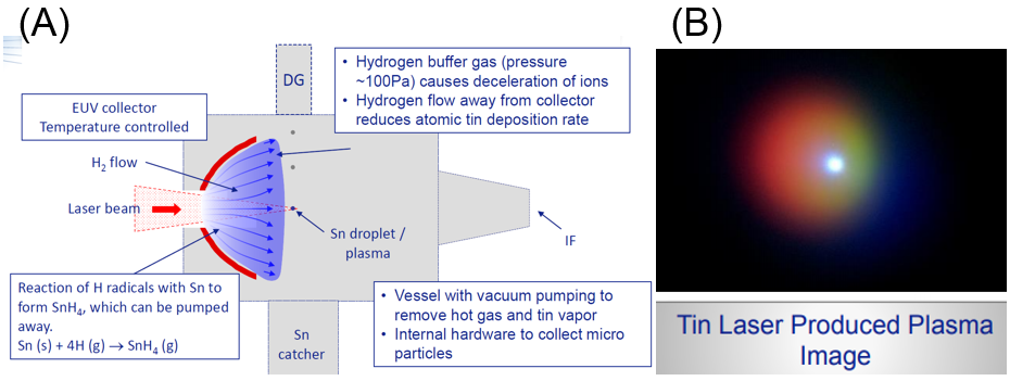
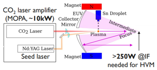
EUV light source power
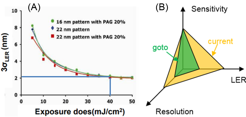
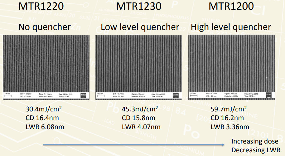
250W light power boosts wafer throughput to 140wph, which makes ASML EUV scanner ready for HMV. Next generation EUV source with further increased EUV energy power, improved conversion efficiency and better dose control is under development, not only to raise wafer throughput but also to further minimize LER which is closely related to dose on wafer. It was found 40mJ/cm2 dose (compared with 20mJ/cm2 from current module) can dramatically reduce LER to smaller than 3nm. 400W EUV source will be implemented in next module of ASML NXE scanner soon. High power EUV is also critical to next generation high NA scanner.
Mirror and reticle defectivity
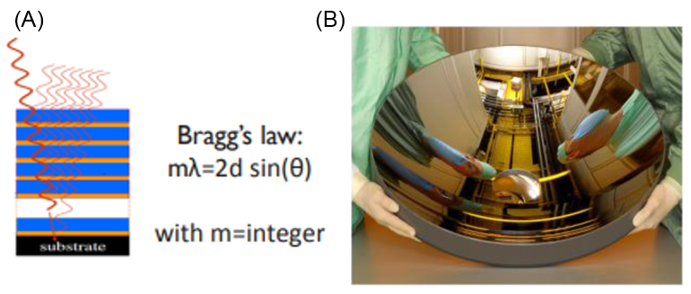
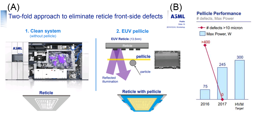
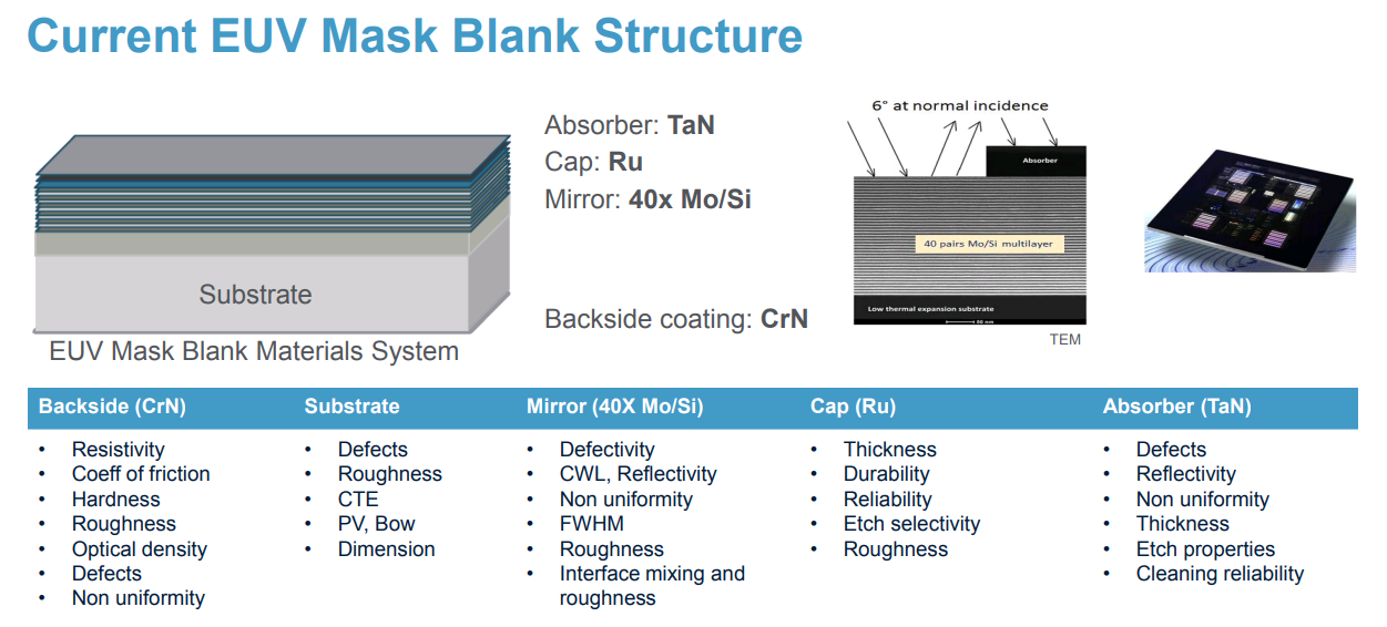
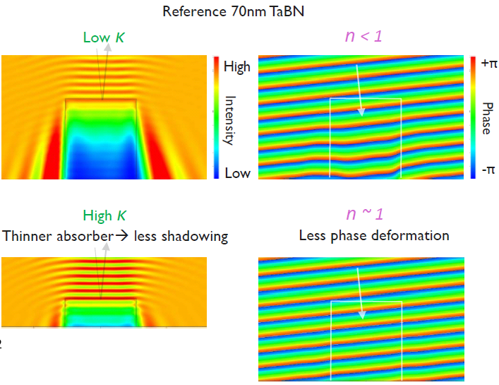
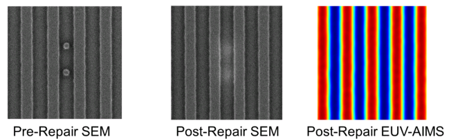
Impurities, thickness inhomogeneity of multilayer mirrors and reticles can change EUV light intensity or phase which will generate defects on wafer. Reticle surface roughness also contributes to LER. Besides superb quality fabrication of multilayer mirrors and reticles, the control of contamination and particles in vacuum chamber is also a big concern since there is no clean pressure gap protection in the reflection chamber and high energy natural of EUV. With the introduction of pellicles and DGL membrane, chamber defects have been reduced to a very low level. In order to detect not only surface impurities but also light phase changes due to internal defects, AIMS inspection system has been developed by ZEISS together with SEMATECH. This tool could check wafer aerial image and detect potential pattern failure on wafer.
LER and CD variation
Compared with deep UV lithography, line edge roughness is much worse for EUVL due to relatively low dose and secondary electron diffusion (stochastic effect). New photo resists such as metal-oxide with polymer ligands are being developed, lithography process flow has been optimized, and reticle flatness is well-controlled, all efforts have successfully reduced the LER to an acceptable level for an ASML EUV system. Further investigation is trying to reduce LER to below 3nm for 3σ from current 3.5nm range from inorganic resist and 5nm range from CAR.
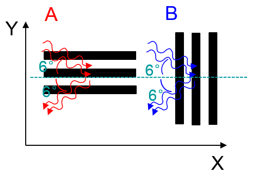
Mask 3D effect
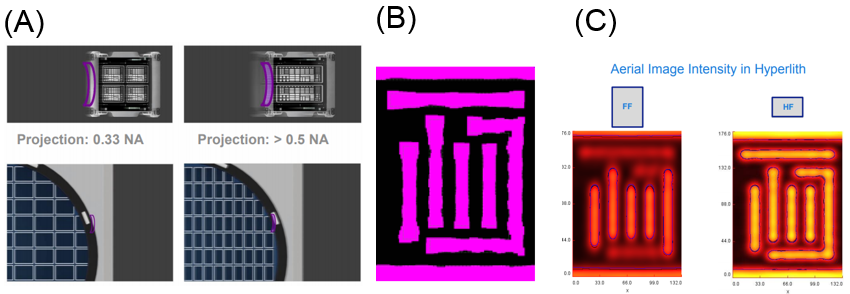
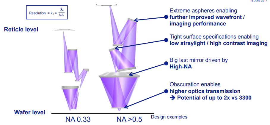
Due to absorber thickness and the chief-ray angle of incident EUV light onto the mask, horizontal and vertical features show different imaging behavior and critical dimension change on wafer, this is called shadowing effect. Mask 3D is also related to reticle blank flatness and bow, multilayer EUV reflectivity, and absorber properties. These effects will decrease the margin of process window with a reduced or shifted depth of focus (DOF). By introducing phase control SMO and OPC correction, orientation-dependent mask CD bias could be compensated. High-k absorbers are also under development to help further reduce shadowing effect. In next generation of high-NA EUV scanner, anamorphic half filed reticle will be introduced to overcome x-y asymmetry and improve throughput[56], but with the cost of design, OPC and mask complexity.
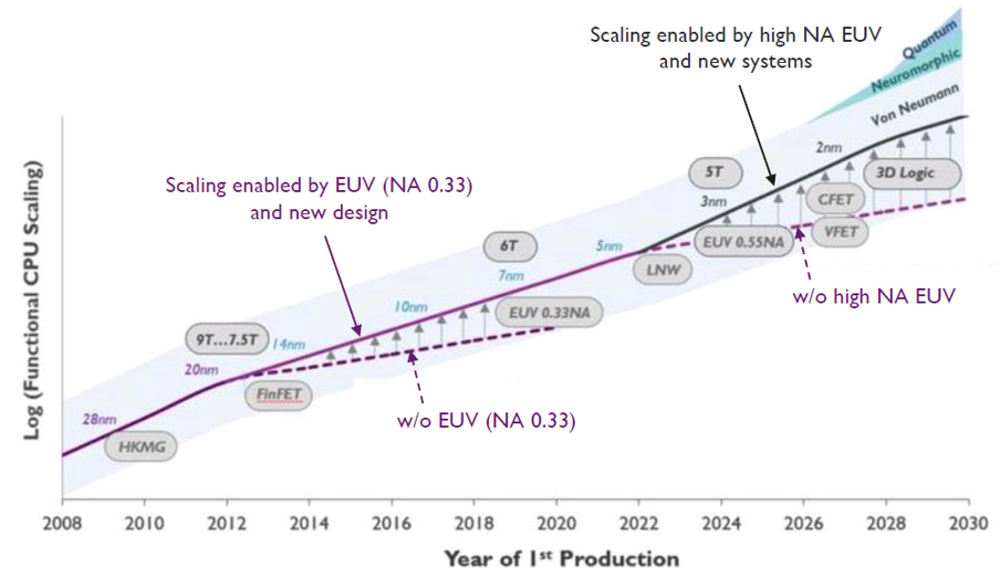
EUVL has achieved great progress since 2015, most of breakthroughs take place after the formation of EUV industry alliances among big player like ASML, INTEL, TSMC and SUMSANG. Industry requirements combined with strong financial support finally drive this technology into HVM. As the only EUVL scanner commercial provider, ASML is going to sell over 30 EUV modules in 2019. The market is ramping up and this revolutionary technology will lead the industry to the next decade[57] (Figure 18).
Figure 18. Technology node scaling is driven by the development of lithography and DTCO. High NA EUV will lead the industry in next decade[14]. Courtesy of Vu Luong, IMEC