Research Article Archive Versions 6 Vol 1 (2) : 18010201 2018
Download
Preparation of Double-sided Nanostructure Based on Soft-nanoimprinting Lithography
: 2018 - 11 - 08
: 2018 - 12 - 12
1943 32 0
Abstract & Keywords
Abstract: Double-sided nanostructure has more excellent properties in high efficiency, high yield, and high capability devices, which becomes the attention spots in nanofabrication technology. We proposed a very simple method to fabricate the double-sided nanostructure on polymer elastic substrate. By using twice soft-nanoimprinting process, the same or different nanostructures array was fabricated onto the elastomeric slab substrate. In this paper, we fabricated double-sided nanopillars array with different diameters of 200nm and 350nm. In order to expand the applications field in optical and electronic devices, metal layer could be deposited onto the substrate before imprinting nanostructure.
Keywords: Double-sided nanostructure, elastic substrate, soft-nanoimprinting lithography, metal layer.
1. Introduction
With the continuous maturity of micro-nano processing technology, the broad application value and prospect of micro/nano-structure materials are becoming more and clearer[1,2]. Micro/nano-structure materials have an important role in electronics, biology, chemistry, optics and mechanics[3-6]. As the feature size of nanostructure continues to shrink, the demand for the functionality of optical and electronic devices is increasing, such as efficiency, storage, capability, size, and cost. Therefore, 2D nanostructure tends to develop 3D nanostructure [7,8].
Compared to 2D nanostructure, the fabrication of 3D nanostructure is more difficult. As a kind of quasi-three-dimensional structure[9,10], double-sided nanostructures display advantages combining the simple preparation of 2D structure and better performances of 3D structure, for example, more flexible and sensitivity. Double-sided nanostructures became the research hot spots. So, the preparation of the double-sided nanostructures is our study fields.
In 2010, P. Granitzer et al. proposed double-sided mesoporous silicon with embedded quasi-regular nanostructures using electrode position[11]. In 2014, C. Zha et al. demonstrated the double-sided brush-shaped TiO2 nanostructure by self-assembly technology[12]. In 2015, I. Mohacsi et al. presented a novel method to fabricate high resolution double-sided nanostructures for hard X-ray microscopy[13]. The researchers used the double-sided zone plates with 30nm smallest zone width to offer up to 9.9% focusing efficiency at 9 keV. These researchers show that the double-sided nanostructures become more and more useful, but the study about double-sided nanostructures on the elastic substrate was little. Furthermore, the fabrication methods were not easy to apply to high yield with low cost.
Based on the abovementioned situation, we present a simple method to make double-sided nanostructures on the elastic substrate by soft-nanoimprint lithography. Soft-nanoimprint lithography is a low pressure technique when contact with flexible film substrate[14,15]. During the fabrication process, we can choose same or different master molds to make double-sided devices with same or different nanostructures. Using the low cost and simple method, we fabricated a double-sided nanopillars array with different diameters of 200nm and 350nm. The double-sided nanostructures have wide applications same as the single side, and the applications could be further expended through depositing metal onto the substrate or nanostructures surface. The double-sided nanostructures with elastic substrate could support advances in flexible optical displays in smart phones and televisions, wearable photonic devices, and ultrasensitive sensors that measure strain.
2. Fabrication Process
The required structures are typically fabricated either by electron beam lithography in a serial fashion over limited areas with imperfect spatial coherence, or by expensive, advanced forms of projection mode photolithography. The soft stamps with nanostructures were fabricated via a simple, soft imprinting procedure in Figure 1. Casting and curing a prepolymer of poly(dimethylsiloxane) (PDMS) against a master of photoresist on silicon wafer, patterned by projection mode deep ultraviolet lithography, formed the soft stamps according to the following procedures. The stamp was prepared as a belayed hard PDMS to reproduce accurately the master’s features, soft PDMS to provide a flexible support for the soft stamp.
The hard PDMS was prepared by mixing base and curing agent at a ratio of 5:1, and the soft PDMS was then poured onto the hard PDMS, prepared by mixing base and curing agent at a ratio of 10:1. The typical thickness of the hard PDMS directly contract with master surface was 10 ~ 20μm, and the soft PDMS was about 2~3mm. Baking at 80℃ for 2 hours completed the curing of the polymers. Releasing the composite PDMS stamp from the master mold, the soft stamp was prepared. Such soft stamps with different nanostructures were preparation from master mold, and each stamp can be used many times. In order to be used as the soft-nanoimprint stamp, the thiol-ene feature must be treated by the surface anti-adhesion agent.


Figure 1.   Soft stamp fabrication process: (a) imprinting, (b) curing, (c) removing.
The fabrication scheme of the double-sided nanostructures on the elastic substrate is shown in Figure 2. In order to easily release from the soft stamp, polyethylene terephthalate (PET) was the elastic substrate. The UV-curable resist was coating onto the PET surface to form a thin film. The composite PDMS stamp was imprinted on the film. Releasing the stamp after curing under the UV light, the single-sided nanostructures same as the master’s features was obtained. Another side of the substrate was imprinted nanostructures via the same fabrication process. If the double-sided nanostructures is used to be transparent optical devices, the simple twice soft-nanoimprint lithography complete the whole process. If the double-sided nanostructures are used to be electronic electrical devices, metal is deposited onto the substrate surface before the fabricating nanostructures to increase the electrical conductivity.


Figure 2.   The preparation scheme of the double-sided nanopillars with the elastic substrate, (a) preparing the stamp and substrate with resist film, (b) curing under the UV light, (c) obtaining one sided nanopillars after releasing the stamp, (d) preparing another stamp and another sided substrate with resist film, (e) curing under the UV light, (f) obtaining the double-sided nanopillars.
The UV-curable resist was the thiol-ene polymer we prepared[16-18]. The resist was prepared by mixing the poly(mercaptopropyl)methylsiloxane (PMMS) (41.5wt %), ethylene glycol dimethacrylate (EGDMA) (58.1wt %), and 2, 2-Dimethory-2-phenylacetopheneone (DMPA) (0.4wt %) as the photoinitiator. The thiol-ene resist could be cured during 30s under the UV light with the power density of 40W/cm2. Therefore, the preparation method we proposed is high- efficiency and low-cost.
3. Experiments Results
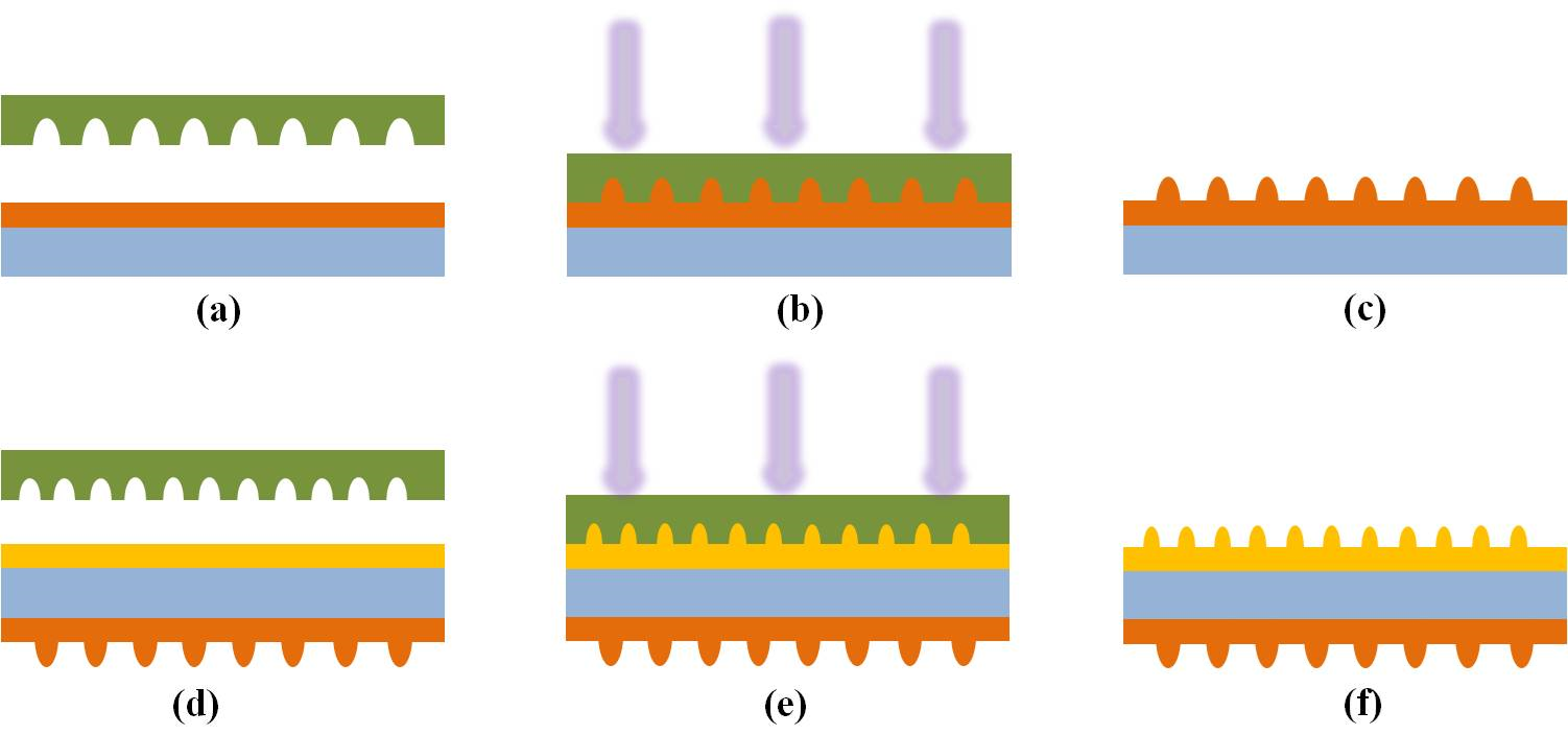
In our experiments, the porous anodic alumina templates were the master molds, which include structures with the diameter of 200nm and 350nm, respectively. The SEM images of the master molds are shown in Figure 3. The nano-hole arrays on the templates were uniform. Two different PDMS stamps were prepared via soft imprinting lithography to be as the soft stamp to fabricate the double-sided nanostrucutres.


Figure 3.   
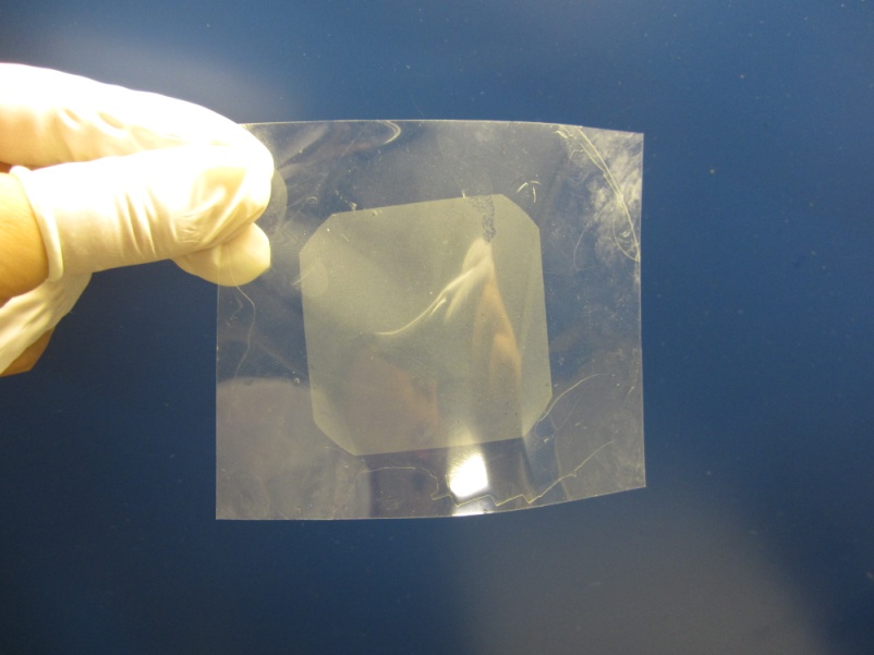
Porous anodic alumina templates: (a) the diameter is 200nm. (b) the diameter is 350nm.
The soft double-sided nanopillar arrays were fabricated via twice soft-nanoimprint lithography as shown in Figure 4. The elastic PET film was the substrate. The large area of the nanopillars array was 3cm×3cm, which was determined by the master mold. The PET we used is transparent for visible light, so the PET double-sided nanopillars array could be used as optical device.


Figure 4.   The photo of the double-sided nanopillars array on the PET substrate.
During the fabrication process, we first used the one PDMS stamp to fabricate the nanostructure on the one side of the PET substrate. The thiol-ene resist was spin-coated onto the surface of the substrate to form a 2μm thick film. Then the stamp was imprinted onto the resist film to make the resist fill into the relief structure. The resist could be cured to form cross-linked polymer under the UV light. Releasing the stamp, the nanopillars array with size of 200nm was achieved, as show in Figure 5(a).
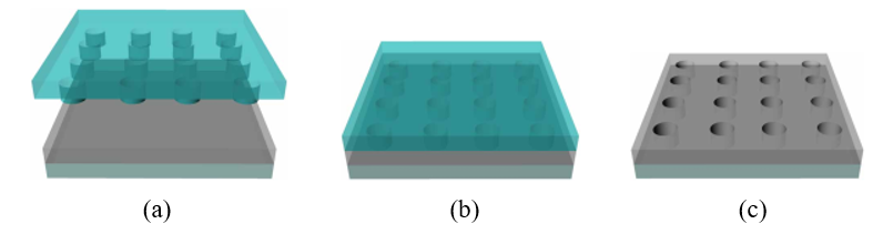
In order to fabricate the nanostructure on another side, a thin PDMS protective film was coated onto the nanopillars array to protect the preparation structures. Because the PDMS film was soft and nonadhesion, it could be gently peeled off the nanostructures without any effects. The same thiol-ene resist was coated onto another side of the substrate via casting process. Because the resist is low viscosity, a uniform 3μm thin film was formed. The other stamp with diameter of 350nm was imprinted onto the film and cured under the UV light for 30 seconds. Releasing the stamp, we obtained the device with double-sided nanopillars array. And the nanopillar with size of 350nm was illustrated in Figure 5(b), which isn’t uniform due to the low performance of the imprint resist and low precision of fabrication process. In future experiments, we will improve the mask and imprint resist to optimize the experimental results.
The nanopillar arrays on the double-sided PET substrate were high-resolution, high uniform and high-precision. The nanopillars array with the diameter of 350nm arranged more densely. In this article, we fabricated nanopillars array with the different diameters. In addition, we could also use two soft stamps with the same nanostructures or completely different nanostructures, such as gratings on the side and nanoholes on another side.
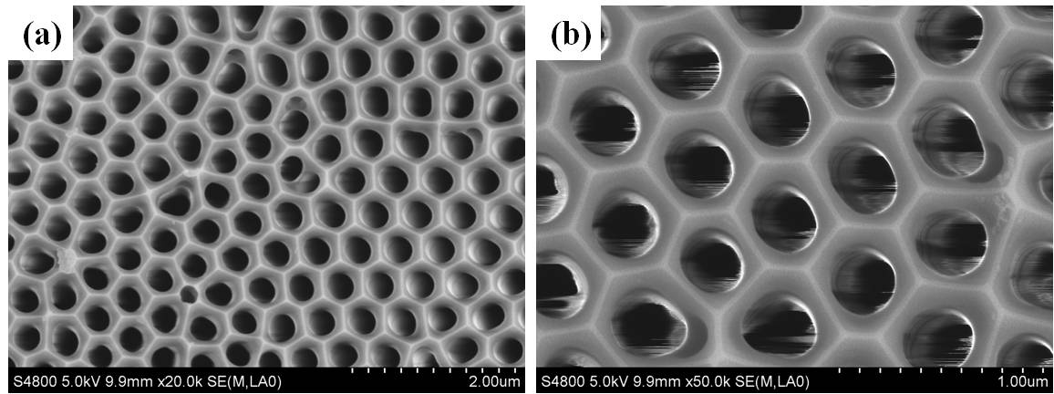
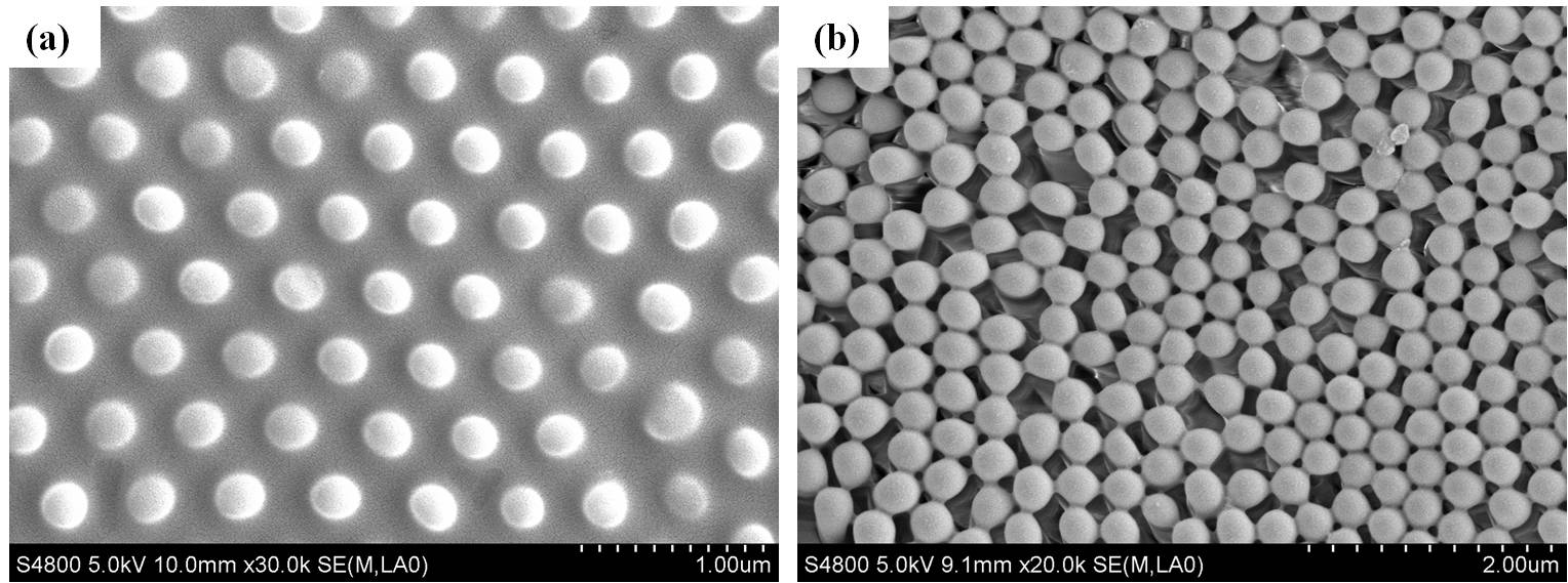

Figure 5.   The SEM images of the double-sided nanostructure on the PET elastic substrate: (a) one sided nanopillars with the diameter of 200nm, (b) another sided nanopillars with the diameter of 350nm.
The UV-curable soft-imprint lithography is very simple, even for fabricating the complicated double-sided nanostructures. The fabrication process is high efficiency, low-cost and high-resolution for inexpensive high-volume commercial production in the future.
As a new kind of quasi-3D nanostructure, the double-sided nanopillars have new capabilities to extend the applications field in optical and electronic devices. For example, in order to enhance the electrical properties, a metal layer was deposited onto the PET substrate. And the antireflection film was coated onto the nanostructures to increase the transmission. Therefore, the double-sided nanostructures have potential on the applications such as nanogenerator, sensor, absorber, and nano-antenna.
4. Conclusion
With the increasing of the applications on optics and electronics devices, 2D nanostructure was developed to 3D nanostructures. Due to the difficulties of fabricating 3D nanostructures, the quasi-3D nanostructures became the key research hot spot. In this paper, we developed a simple method for fabricating double-sided nanopillars on the elastic substrate via soft-nanoimprint lithography. Large-area and high-resolution double-sided nanopillars on the soft substrate was prepared via twice simple soft imprinting processes. Therefore, the new method could be applied to inexpensive high-volume commercial production in the future, especially for the nanoscale optical and electrical components and systems.
Acknowledgements
We acknowledge the financial supports of the National Nature Science Foundation (No.61605211) of China and Science and Technology Support Program of Sichuan province (No.2016RZ0067).
[1]
C. Li, K. Luo, H. Li, et al., “Research progress in the preparation of calcium sulfate micro/nano-structure materials,” Science & Technology in Chemical Industry,17 (4), 57-60 (2009).
[2]
M. Zheng, “Preparation of micro-nano-structure of materials surface and its research process,” Hot Working Technology,40 (24), 145-148 (2011).
[3]
W. Liu, J. Zhang, L. Wan, et al., “Dielectrophoretic manipulation of nano-materials and its application to micro/nano-sensors,” Sensors & Actuators B Chemical,133 (2), 664-670 (2008).
[4]
X. Zhang, F. Cheng, K. Zhang, et al., “Facile polymer-assisted synthesis of LiNi0.5Mn1.5O4 with a hierarchical micro-nano structure and high rate capability,” Rsc Advances,2 (13), 5669-5675 (2012).
[5]
F. Chu, X. Wu, “Fabrication and condensation characteristics of metallic superhydrophobic surface with hierarchical micro-nano structures,” Applied Surface Science, 371 , 322-328 (2016).
[6]
Z. Yi, Q. Han, D. Geng, et al., “One-pot chemical route for morphology-controllable fabrication of Sn-Sb micro/nano-structures: Advanced anode materials for lithium and sodium storage,” Journal of Power Sources,342 , 861-871 (2017).
[7]
H. H. Nersisyan, J. H. Lee, J. R. Ding, et al., “Combustion synthesis of zero-, one-, two- and three-dimensional nanostructures: Current trends and future perspectives,” Progress in Energy & Combustion Science, 63 , 79-118 (2017).
[8]
A. Kodigala, T. Lepetit, B. Kanté, “Exceptional Points in three-dimensional Nanostructures,” Physical Review B,94 (20), 1-5 (2016).
[9]
S. Ito, B. Feng, M. Arita, et al., “Evolution in electronic structures of quasi-three-dimensional Bi films: evidence for nontrivial topology of Bi,” Physical Review Letters,117 (23), 1-6 (2016).
[10]
O. Kemppinen, Y. Heinson, M. Berg, “Quasi-three-dimensional particle imaging with digital holography,” Appl Opt.,56 (13), F53 (2017).
[11]
P. Granitzer, K. Rumpf, M. Albu, et al. “Double-sided mesoporous silicon with embedded quasi-regular arranged ferromagnetic nanostructures fabricated by electrodeposition,” ECS Meeting,25 (27), 139-145 (2010).
[12]
C. Zha, L. Shen, X. Zhang, et al., “Double-sided brush-shaped TiO2 nanostructure assemblies with highly ordered nanowires for dye-sensitized solar cells,” Acs Appl Mater Interfaces,6 (1), 122-129 (2014).
[13]
I. Mohacsi, I. Vartiainen, M. Guizarsicairos, et al., “High resolution double-sided diffractive optics for hard X-ray microscopy,” Optics Express, 23 (2), 776-86 (2015).
[14]
B. Kwon, J. H. Kim, “Importance of molds for nanoimprint lithography: hard, soft, and hybrid molds,” Journal of Nanoscience,2016 (16), 1-12 (2016).
[15]
J. Zhu, Y. Bai, L. Zhang, et al., “Large-scale uniform silver nanocave array for visible light refractive index sensing using soft UV nanoimprint,” IEEE Photonics Journal,8 (4), 1-7 (2016).
[16]
M. Zhang, Q. Deng, L. Shi, et al., “Fabrication of nano-pillar with sub-100nm resolution based on thiol-ene,” Nanophotonics and Micro/Nano Optics II. International Society for Optics and Photonics, 92771U, (2014).
[17]
M. Zhang, L. Xia, Q. Deng, et al., “Nanobowl array fabrication via conglutination process based on thiol–ene polymer,” IEEE Photonics Journal,7 (4), 1-6 (2015).
[18]
M. Zhang, A. Cao, L. Shi, et al., “Fabrication of hybrid soft-nanoimprint mold in benign ambient based on thiol–ene,” Optik - International Journal for Light and Electron Optics,126 (23), 4123-4126 (2015).
Article and author information
Man Zhang
zhangman@ioe.ac.cn
Qiling Deng
Hui Pang
Lifang Shi
Axiu Cao
Publication records
Published: Dec. 12, 2018 (Versions6
References
Journal of Microelectronic Manufacturing