Research Article Archive Versions 1 Vol 3 (1) : 20030102 2020
Download
Metrology Challenges in 3D NAND Flash Technical Development and Manufacturing
: 2019 - 10 - 07
: 2020 - 03 - 30
4309 148 0
Abstract & Keywords
Abstract: 3D NAND technical development and manufacturing face many challenges to scale down their devices, and metrology stands out as much more difficult at each turn. Unlike planar NAND, 3D NAND has a three-dimensional vertical structure with high-aspect ratio. Obviously top-down images is not enough for process control, instead inner structure control becomes much more important than before, e.g. channel hole profiles. Besides, multi-layers, special materials and YMTC unique X-Tacking technology also bring other metrology challenges: high wafer bow, stress induced overlay, opaque film measurement. Technical development can adopt some destructive methodology (TEM, etch-back SEM), while manufacturing can only use non-destructive method. These drive some new metrology development, including X-Ray, mass measure and Mid-IR spectroscopy. As 3D NAND suppliers move to >150 layers devices, the existing metrology tools will be pushed to the limits. Still, the metrology must innovate.
Keywords: 3D NAND; Metrology; Semiconductor; HAR; Process Control
1.   Introduction
Thanks to its storage density and speed, flash memory had changed our lives. SSD (solid state disk) have become much cheaper and trends to replace hard disk. With the growing of big data and cloud storage, the innovation of flash memory must be pushed. As 2D flash technique is hard to scale down due to lithography, 3D flash technique has been developed and evolved very fast these years. 3D NAND fundamentally changes the scaling paradigm: instead of traditional scaling in horizontal plane, 3D NAND scales in the Z-direction by stacking multiple layers vertically. YMTC, as one of 3D NAND flash memory suppliers, already got some progress, 64L production line have been established and will accomplish mass production by end of this year.
The important feature of 3D NAND is the multi-layer architecture with high-aspect-ratio holes (including channel hole and contact hole). The process challenges shift from lithography to film deposition and hole etch. New materials and advanced equipment are being developed.
The straightforward way to visualize process performance is by cross-section TEM, but it is destructive and throughput is a concern. Traditional metrology methods (SEM, OCD, AFM and so on) plays important role during process development and control. Compared to 2D flash structure, process engineer rely much more on metrology results to fine tune their process. Not every lot or wafer goes through metrology steps. When the process is stable, the sampling rate could be low; otherwise sampling rate could be high. Smart sampling is being developed to balance the risk of not measuring versus measuring everything. Timely develop robust metrology recipes affect the success of current and future 3D NAND technical development and manufacturing. It requires professional engineers to maximize its value in the fab.
In the next chapter, we will introduce several metrology techniques, including their advantages and disadvantages. After that, metrology challenges will be introduced. Finally we will introduce X-Tacking and its related metrology requirements.
2.   Metrology Toolsets
2.1.   CD-SEM
The CD-SEM is commonly used by litho and etch process engineer. Similar with other scanning imaging system, CD-SEM controls electron beam scanning by electromagnetic lens and detects signal (SE & BSE) at each pixel. An image is constructed through software, along with some image process algorithm to calculate critical parameters. The SEs have relatively low energy (<50eV), while BSEs have relatively high energy (>50eV). Typically SEs carries surface topology information, while BSEs carry material-contrast information. The inline CD-SEM resolution is about 1~2nm [1].
The major advantage of CD-SEM is that the measurement is quite straightforward, and diagnose is easy as long as images are saved. However, CD-SEM cannot meet all 3D measurement requirements, like under-etch and trench height. Tilting beam may enable CD-SEM to measure vertical dimension, but the precision could be an issue and need further investigation. Besides, electron interacts with material being measured and sometimes induces damage phenomena. Resist is quite sensitive and need avoid repeating measure.
2.2.   Optical Film and CD
Two of most common optical techniques are reflectometer and ellipsometer. Both are model-based and indirect measurement (instead of direct measurement, such as CD-SEM). The signal comes from film thickness, film characterization (n&k) or patterned structures, which introduces the changes of reflected light’s property. The original raw data (called spectra) is the intensity over wavelength at different subsystem. Reported results are calculated from a model/library based on some regression algorithms, to minimize the difference between measured spectra and calculated spectra. Fitting indicator (GOF or chi-square) is also included in the result and provide further diagnostic information.
Scatterometry [also called optical critical dimension (OCD)] collects diffraction optical signal from periodic grating. Most of scatterometry tools share same hardware with optical film tools, thus the measured spectra is collected in the same way with optical thin film tools. However, scatterometry process the measured spectra is a different way-library based regression. A library is generated beforehand based on an optimized model. This methodology can reduce inline calculation time a lot. In order to obtain the best model, engineer must do plenty of iteration to check the model output, and this is the most time-consuming step in OCD work flow.
The major benefit of optical technique is the high throughput and non-destructive. It can provide lots of information, including film thickness, CD and SWA. And the key challenges of scatterometry are long library setup time and requirement for reference data to check the model accuracy. Besides, correlation among multiple parameters (thickness, CDs) produces lots of measurement uncertainty, as their impact on reflected spectra is quite similar and cannot be separated [1].
The common trend of optical technique is adding more subsystems/channels to get more information that potentially help improve sensitivity or reduce correlations. It includes multi-AOI, multi-azimuthal angle, longer wavelength, Mueller matrix and so on. However, more subsystems make tools more complex, slow and expensive. [1]


Figure 1.   Block diagram of the scatterometry technique. [1]
2.3.   MBIR (Model Based Infrared Reflectometry)
MBIR is another optical metrology that has been introduced for measure thick film thickness and periodic structures. When measuring patterned structures, they are modeled as multi-layers with effective medium approximation (EMA) [2].As shown in Figure 2, the hole structure is modeled as film layer mixed by background material and void. Absolutely this technique cannot tell x-direction and y-direction CDs, instead it only calculate area. Similar with scatterometry, MBIR solves inverse problem, which means parameters are optimized to minimize the delta between collected spectra and simulated spectra. But MBIR calculation is faster, the simulated spectra can be calculated rapidly using Fresnel Equations [2]. This brings an advantage to MBIR, short recipe turnaround time. It does not need generate a library as scatterometry does. MBIR utilize infrared (1um to 20um) optical system, the precision could be a problem and need more studies.


Figure 2.   MBIR model.
2.4.   MASS Metrology
The concept is very simple-measure the weight. Most semiconductor processing steps involve the addition or removal of material, so wafer mass has direct response to process variability. To measure the mass change with enough fidelity, the system has to overcome several environment factors’ impact and keeps high mass resolution. Furthermore, in many applications, the sensitivity of mass measurements increases with high aspect ratio, perfectly suitable for 3D NAND process, imaging that the volume of material is increased a lot when being deposited in a deep hole than on top of a plane. This methodology can measure almost everything, as long as mass resolution meets its requirement. However, the intrinsic limitation of mass metrology is that it cannot monitor within wafer variations.
2.5.   XPS (X-ray photoelectron spectroscopy)
XPS is being adopted in the production and development of 3D NAND, after its success of measuring high-k material thickness in logical devices. XPS is mainly a surface analysis technique based on photoelectric effect-Electrons are ejected from film surface after X-ray photon irradiation. By XPS energy analyzer, electron counts versus binding energy are plotted. The peak intensity provides the thickness of the film. Quantitative analysis needs a reference peak (typically refer to silicon peak) and calibrations. XPS cannot measure film thickness greater than ~10nm, as electrons at deep location cannot escape from material surface [3].
3.   Metrology Challenges
3.1.   Channel Hole Profile.
Channel hole etch is the most critical process step in 3D NAND flash technical development and manufacturing. Any abnormity would impact post-steps: such as block/trap/tunnel layers deposition and channel formation, finally affect cell function and reliability. Besides, the uniformity is extremely important for process control, thus channel hole related parameter control spec is very tight. Engineers are willing to visualize the whole profile, not only in R/D phase but also in mass production phase. Those critical parameters include CD variations at top and bottom, bowing, under-etch, twisting, tilting and so on. (See Figure 3)


Figure 3.   Channel Hole Etch Challenges (Lam Research).
It is highly expected that CD of each WL (word line) can be measured. But this can only be achieved by destructive methods: cross section TEM or Etch back CD-SEM. Currently OCD serves as the main non-destructive methodology for inline CH (channel) etch CD measurement. As layers number increase, it brings lots of challenges for OCD.
CDs number. Too many floating parameters will make the model very complex and computation time increased exponentially. Actually it is not feasible for 3D NAND structures. Due to 3D NAND development roadmap, the depth of channel hole is doubled at each node transition, making the sensitivity of bottom CDs too weak. Meanwhile, CDs of neighboring WLs gives same spectra response, and cannot be differentiated. This problem is called modeling correlation issue. Typically bottom CDs are coupled with middle CD, to increase model stability. But this makes bottom CDs measurement not always correct and bring risks when the relation between middle CDs and bottom CDs changed.
Robustness and cycle time. 3D NAND modeling is very struggling, as there are thousands of parameters. Modeling has to do lots of assumptions: 1) All oxide tier layers are constrained to one thickness; 2) Hole CDs are exactly same during one repeating unit; 3) CD shape is a circle or ellipse. These modeling errors have to be compensated by other parameters, e.g. material dispersion. It takes long time (>1 week) to get fitting. Sometimes, modeling scientist has to simply the model to reduce calculating time but bring modeling error more or less. OCD often fail the accuracy test by being correlated to TEM, after CD profile change or pre-step changes. Often engineers suffer from OCD tuning until the process is stable. Besides, cycle time of each tuning is too long, >=1 week after TEM results are ready, while process engineers need know the tuning results immediately. Thus OCD is hard for using during channel hole etch R/D phase. Though all vendors are optimizing their calculating algorithm to reduce cycle time, but still this is a bottleneck for OCD.
MBIR is being evaluated to measure hole CDs. Compared to OCD, MBIR model is quite simple with EMA model. As shown in Figure 2, hole structure is modeled as transition layer combing background material and void. The calculation time is very short (at the level of optical film technique) as it is based on Fresnel equations. Thus short cycle time is one advantage for MBIR. However, its performance needs further investigation.
We studied measuring HMO (hard mask open) CDs by MBIR. HMO is previous step before channel hole etch. From the results, it can achieve good correlation with TEM (Figure 4), but precision results is 4X worse than OCD, due to infrared optical system. Compared to process monitor requirement, the precision performance is quite marginal (Figure 5).


Figure 4.   HMO MBIR CDs results. (Correlations with TEM).


Figure 5.   HMO MBIR Precision Performance.
3.2.   Ultra-Thin Film in-line Measurement
3D NAND flash memory’s channel hole is filled by blocking-trapping-tunnel film, namely ONO films. The thickness of ONO films has to be controlled precisely as it is directly related to device performance, including threshold voltage and data retention. For quite a long time, the monitoring is being conducted on dummy wafers (without patterned structures) which are processed together with production wafers. However, there are loading effects that make dummy wafer performance not always show same behavior as production wafers. In-die measurement is required. Nominal value of ONO is very small (<10nm), the requirement for metrology is quite aggressive. A measurement with <0.1nm precision is required.
The conventional method to measure thin film is reflectometer and ellipsometer (optical technique). The big challenge of ONO film is that the optical property of oxide and nitride is quite similar and cannot be differentiated clearly. Besides, ONO thin films are deposited on thick oxide/multi-layers; background noise makes ONO measure variation larger and not being accurate. Data feed forward may be one strategy but is hard to be implemented.
XPS is surface analysis technique and is expected to reduce background layers disturb. The basic principle of XPS is to analyze peak intensity of specified bond energy. Typically quantitative analysis is based on comparing peak of interest to Si-Si peak intensity. However, this cannot be achieved in inline trapping layer measurement, because the underlying layer is oxide. Actually trapping layer is not pure nitride but SION instead; the N/O ratio also has impact on peak intensity, making the recipe very complex and need further investigation.
Mass metrology turns out to be a good choice, as measurement location shift from unpatented wafer to patterned structure. 3D NAND flash has a deep hole structure, the sensitivity of depo film mass versus film thickness is greatly improved by 10X (Lam Research). The precision (3sigma) of mass metrology is around 100ug, which is equivalent to ~0.02nm film thickness and meet process control requirement. However, the limitation of mass metrology is that it cannot monitor WIW uniformity.


Figure 6.   ONO deposition illustration. a)Channel Etch; b) nitride depo in channel; c) nitride dep on film pad.


Figure 7.   Mass sensitivity to film thickness. (blanket vs patterned wafer)(Lam Resarch).
3.3.   Thick and Opaque Film
As device manufacturers move to 256 layers and beyond, new improvements in the system are being developed to deal with very thick and opaque film. An opaque material (k=0.3~0.7 during visual wavelength region) is used for hard mask film and its thickness maybe over 3um. It’s difficult to use traditional SE & SR method to measure very thick film & opaque film. Currently, the wavelength of optical metrology tool is around 200nm~ 2000nm. It’s difficult to penetrate very thick film. The infrared spectroscopy is introduced because of its longer wavelength. The model based infrared spectroscopy involves measuring the spectral reflectance of a surface in a range between approximately 1 and 20 microns. This hard mask film is usually transparent at infrared wavelength range. An alternative method to monitor thick and opaque film is mass metrology, but within wafer variation cannot be measured.
3.4.   Dual Deck
As 3D NAND move to 128 layers and beyond, dual deck and even multi decks could be introduced. These HAR structure process has many parameters need to be controlled, of which dual deck overlay is new and very challenging. More studies need be conducted by optical technique or HV-SEM, or new X-ray metrology.
4.   X-Tacking
Continued manufacturing process improvements are essential in delivering memory devices with higher I/O performance, higher bit density, and at lower cost. Current 3D NAND technology involves process steps that form array and peripheral CMOS (Complementary Metal-Oxide-Semiconductor) regions side-by-side, resulting in waste of silicon real estate thermal budget deficit and film stress compromises, thus limits the paths of making advanced 3D NAND devices. An innovative architecture was invented to overcome these challenges by connecting two wafers electrically face-to-face through metal VIAs (Vertical Interconnect Access).
Traditional approach to connecting wafers is by using VIA, but metal in the VIA exhibits higher coefficient of thermal expansion (CTE) compared to silicon and dielectrics in the wafer, and this induces large stresses in both the metal plugs and the surrounding silicon. The large thermo-mechanical stress can be mitigated by proper CMP (Chemical Mechanical Planarization) process. In a study of a CMP process resulting in VIA shape that is slightly protruding on the top wafer and slightly dishing in the bottom wafer, thus allowing for necessary wafer to wafer overlay bonding tolerance, better overall resistivity and yield were achieved [4].
Wafer bonding, as a 3D integration technology, provides a new paradigm to vertically integrate various building blocks. Not only can it shorten wires with smaller chip sizes, but also it is a new technology platform for heterogeneous integration by stacking and connecting dissimilar materials or different modules on one substrate. Today, the pre-bonding wafer-to-wafer alignment accuracy can be achieved on the order of 0.25 μm using commercially available wafer-to-wafer alignment tools [5, 6]. However, the process related misalignment has yet to be thoroughly studied, while it becomes more significant.
Highly accurate and efficient metrology is required to monitor interface processing and wafer connecting procedures due to increased process complexity and precision requirements. Universal metrology and measurement techniques are applied here include ellipsometry for thin film thickness and corresponding wafer-wide variation, SEM for VIA critical dimensions, AFM for interface roughness, profilometry for interface topography and IR transmission microscopy for bonding misalignment. Advanced metrology technologies have been developed for related processes controlling, however more insights must be given to solve systematic bottlenecks and meet the request of higher production throughput. Basically improvements are in dire need in two parts:
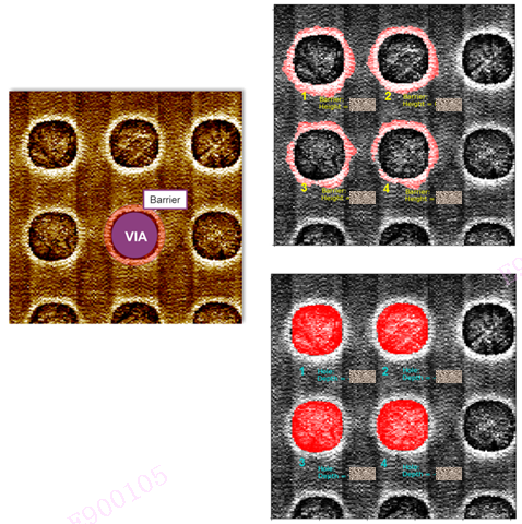
VIA Dishing -The VIA interface topography, which normally resembles a dishing shape to ensure connection between wafers, is one of the most important factors in determining the quality of wafer interconnection. A suitable monitoring scheme for VIA dishing is necessary to avoid structural and reliability issues such as interconnection open, metal void, metal diffusion, etc. The industry has developed several methods in the product development flow to proactively identify these hotspots, also known as weak points [7-9]. Despite all such design verification methods, we must still employ aggressive metrology methods to detect any deformation during fabrication [10, 11]. AFM appears to be the only reliable metrology method for this purpose. Yet it still poses two primary metrology challenges. Firstly, the shallow depth makes it difficult for capturing the edges of these VIA features on wafer. Frequent capturing failures happen when measuring VIA dishing because of the small average depth. Also, partial capturing and unwanted pixels exacerbate the difficulty in accurate measurement. Secondly, the dishing depth varies depending on metal volume and density distribution that is caused by chip layout, which leads to potential weak points. To address the problems, our previous work (Figure. 8) demonstrated the implementation of an inline metrology to precisely measure VIA location and its depth of dishing and protrusion, ensuring better CMP process control by utilizing pattern centric solution [12].


Figure 8.   (Left) original AFM data shows metal barrier around VIA; (right-top) barrier height and (right-bottom) dishing depth was automatically exported by the IDP application based on VIA sequence.
Yet the long measurement duration severely limits the application of AFM in mass production [13]. Among height related measurement methods, WLI (White Light Interferometer) offers an alternative option. In brief, white light interferometer provides high precision by using optical phase-shifting techniques, and a broad spectral width light source is generally applied in order to increase dynamic range of measurement [13]. Although a vertical scanning is mandatory to collect interference fringes, the field data with less than 100 nm per pixel resolution is obtained spontaneously by WLI, which greatly reduces measurement duration. As a result, WLI is more than 100 times faster than line-scanning AFM in the same measurement. But multiple-layer reflection caused by transparent films stack has a large impact on the interference fringes since it shifts the wave phase and derives inauthentic height. For improvement, a spectrometer which measures spectrum with high precision at the reference location of the test surface can be added to a typical WLI optical system for pattern sample topography measurement [14].
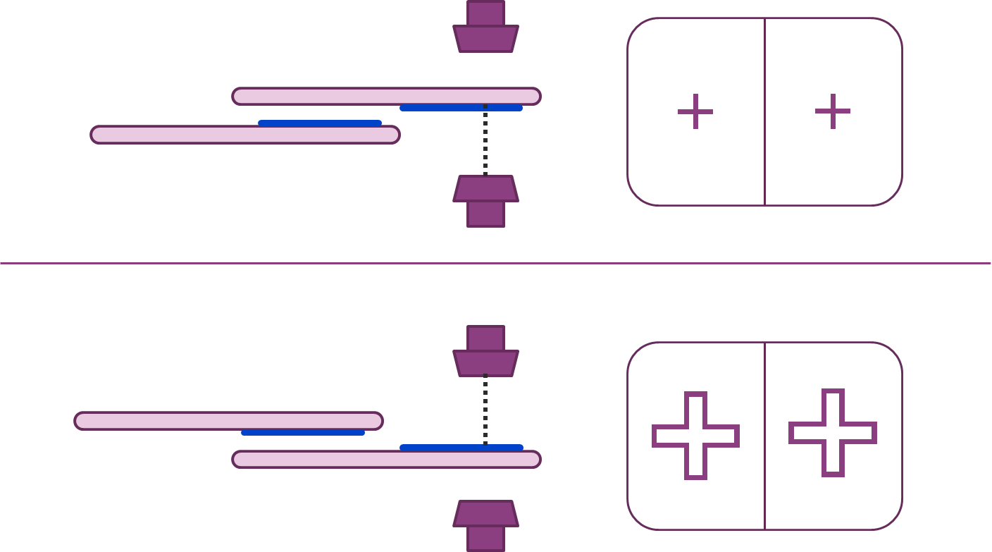
Misalignment -Compared to conventional mask-to-wafer alignment based on photolithography, wafer-to-wafer alignment is much more complicated. It requires different alignment concepts to align two processed wafers with devices. In principle, wafer-to-wafer alignment uses alignment marks on two wafers to monitor the alignment process within an alignment tool. Once two wafers are aligned, they are temporarily brought into contact; at this stage, for optical or infrared (IR) transparent wafer, the misalignment can be inspected by imaging overlay marks.
Various alignment techniques and methods have been introduced for wafer-to-wafer alignment, among which the method called SmartView [15, 16] is widely applied. Two pairs of microscopes are placed outside of the top and bottom wafers. The aligning wafers are placed “face-to-face” with a gap of less than 100 μm and vacuum-sucked on the top and bottom wafer stages, respectively. The two wafer stages can be moved back and forth horizontally. After the pair of top and bottom microscopes are aligned with each other (i.e., calibrated), the bottom wafer stage is moved in between the pairs of microscopes; the marks in the top microscopes are aligned to the alignment marks on the bottom wafer. The bottom wafer position is stored, and the bottom stage is retreated. The top wafer stage is moved to the position against the bottom microscopes. The alignment marks on the top wafer are then aligned to the bottom microscopes. The bottom wafer stage is moved back to its stored alignment position. Finally, the two aligned wafers are vertically moved to contact each other and are clamped to hold the alignment for wafer bonding, as illustrated in Figure 2. Misalignment tolerances can be achieved on the order of 0.25 μm in this method.


Figure 9.   SmartView alignment method.
As 3D NAND design VIA size and pitch is scaling down to sub-micro in order to increase memory intensity, misalignment needs to be compressed down to 0.1 μm, raising a major challenge for bonding equipment suppliers. Currently main movement is striving to improve measurement repeatability and to apply feed forward method to compensate bonding misalignment.
5.   Summary and Outlook
Metrology stands out as a great challenge as 3D NAND flash technique is being developed. New materials and new structure design both bring out new challenges. Metrology engineer has to be more and more professional, to select most proper methodology. Often one single metrology technique cannot meet requirement, hybrid metrology will be introduced, using two or more toolsets to measure aspects of the same sample. Data from one toolset is exchanged with another to enhance the measurement performance [1].
Acknowledgments
The authors would like to thank all YMTC metrology vendors for helping with tool evaluation, data collection and data analysis.
[1]
Bo Su, Eric Solecky, Alok Vaid, “Introduction to metrology applications in IC manufacturing”, SPIE Press, 2015.
[2]
Zhang, Chuanwei, Liu, Shiyuan, Shi, Tielin, Tang, Zirong. (2009). Improved model-based infrared reflectrometry for measuring deep trench structures. Journal of the Optical Society of America. A, Optics, image science, and vision. 26. 2327-35. 10.1364/JOSAA.26.002327.
[3]
Mainul Hossain, Ganesh Subramanian, Dina Triyoso, Jeremy Wahl, Timothy Mcardle, Alok Vaid, A. F. Bello, Wei Ti Lee, Mark Klare, Michael Kwan, Heath Pois, Ying Wang, Tom Larson, "XPS-XRF hybrid metrology enabling FDSOI process," Proc. SPIE 9778, Metrology, Inspection, and Process Control for Microlithography XXX, 97780N (24 March 2016).
[4]
Takeyoshi Ohashi, Atsuko Yamaguchi, Kazuhisa Hasumi, Masami Ikota, Gian Lorusso, Chi Lim Tan,Geert Van den bosch, Arnaud Furnémont, “Precise measurement of thin-film thickness in 3D-NANDdevice with CD-SEM,” J. Micro/Nanolith. MEMS MOEMS 17(2), 024002 (2018), doi: 10.1117/1.JMM.17.2.024002.
[5]
Eric Beyne, Soon-Wook Kim, Lan Peng, Nancy Heylen, Joke De Messemaeker, Oguzhan Orkut Okudur, Alain Phommahaxay et al. "Scalable, sub 2μm pitch, Cu/SiCN to Cu/SiCN hybrid wafer-to-wafer bonding technology." In Electron Devices Meeting (IEDM), 2017 IEEE International, pp. 32-4. IEEE, 2017.
[6]
B. Kim, T. Matthias, M. Wimplinger, and P. Lindner, “Advanced wafer bonding solutions for TSV integration with thin wafers,” in Proc. IEEE Int. Conf. 3D Syst. Integr., San Francisco, CA, Mar. 2009, pp. 1–6.
[7]
H. W. van Zeijl and P. M. Sarro, “Alignment and overlay characterization for 3D integration and advanced packaging,” in Proc. 11th EPTC, Dec. 9–11, 2009, pp. 447–451.
[8]
Gyun Yoo, Jungchan Kim, Taehyeong Lee, Areum Jung, Hyunjo Yang, Donggyu Yim, Sungki Park, Kotaro Maruyama, Masahiro Yamamoto, Abhishek Vikram, Sangho Park, "OPC verification and hotspot management for yield enhancement through layout analysis", Metrology, Inspection, and Process Control for Microlithography XXV, Proc. of SPIE Vol. 7971, 79710H, 2011.
[9]
Taehyeong Lee, Hyunjo Yang, Jungchan Kim, Areum Jung, Gyun Yoo, Donggyu Yim, Sungki Park, Akio Ishikawa, Masahiro Yamamoto, Abhishek Vikram, "Hot spot management through design based metrology: measurement and filtering", Proc. SPIE. Vol. 7520, 75201U, 2009.
[10]
Eric Guo, Shirley Zhao, Sandy Qian, Guojie Cheng, Abhishek Vikram, Ling Li, Ye Chen, Chingyun Hsiang, Gary Zhang, Bo Su, "Simulation based mask defect repair verification and disposition" Proc. of SPIE Vol. 7488, 74880G, Photomask Technology, 2009.
[11]
Jing Zhang, Qingxiu Xu, Xin Zhang, Xing Zhao, Jay Ning, Guojie Cheng, Shijie Chen, Gary Zhang, Abhishek Vikram, Bo Su, "Yield impacting systematic defects search and management", Design for Manufacturability through Design-Process Integration VI, Proc. of SPIE Vol. 8327, 832716, 2012.
[12]
Abhishek Vikram, Kuan Lin, Janay Camp, Sumanth Kini, Frank Jin, Vinod Venkatesan, “Inspection of high-aspect ratio layers at sub 20nm node”, Metrology, Inspection, and Process Control for Microlithography XXVII, Proc. of SPIE Vol. 8681, 86811Q, 2013.
[13]
Sicong Wang, Jian Mi, Abhishek Vikram, Gao Xu, Guojie Chen, Liming Zhang, Pan Liu, "Novel pattern-centric solution for high performance 3D NAND VIA dishing metrology", Design-Process-Technology Co-optimization for Manufacturability XIII, Proc. of SPIE Vol. 10962-42, (2019).
[14]
Chen, Jianchao. "Comparison of optical surface roughness measured by stylus profiler, AFM, and white light interferometer using power spectral density." Proc Spie 7656.2(2010).
[15]
Xiaoye Ding, Sicong Wang, Yi Zhou, Yanzhong Ma, Le Yang, Chi Chen, “White Light Interference Solution for Novel 3D NAND VIA Dishing Metrology”, unpublished.
[16]
W. H. Teh, C. Deeb, J. Burggraf, M. Wimplinger, T. Matthias, R. Young, C. Senowitz, and A. Buxbaum, “Recent advances in submicron alignment 300 mm copper-copper thermocompressive face-to-face wafer-to-wafer bonding and integrated infrared, high-speed FIB metrology,” in Proc. IEEE IITC, Burlingame, CA, Jun. 6–9, 2010, pp. 1–3.
[17]
S. Farrens, “Wafer and die bonding technologies for 3D integration,” in Proc. Mater. Res. Soc. Symp., Boston, MA, 2008, vol. 1112, p. 1112-E01-06.
Article and author information
Wei Zhang
Andrew_Zhang@ymtc.com
Jun Xu
Sicong Wang
Yi Zhou
Jian Mi
Publication records
Published: March 30, 2020 (Versions1
References
Journal of Microelectronic Manufacturing