As summarized from publication, the basic design rules are listed in Table 1, as follows. The fin pitch follows a trend shrinking from 33~42 nm at 10 nm node to 27~30 nm at 7 nm node, and to about 22.5~25 nm at the 5 nm node. The gate (poly) pitch shrinks from 66~68 nm to 54~56 nm, and 44~50 nm from 10 nm to 7 nm, and to 5 nm, respectively. And the metal pitch from 44~48 nm, to 36~40 nm, and to 30~32 nm pitch, respectively, from 10 nm to 7 nm, and to 5 nm. It is noted that the ratio of shrink between generations is around 0.8~0.85. Here, we pick a minimum fin pitch of 22.5 nm, minimum poly pitch of 50 nm and a minimum metal pitch of 30 nm. The reason for the poly pitch of 50 nm is due to difficulty in high-K dielectric deposition and work function metal deposition into narrow gate length.
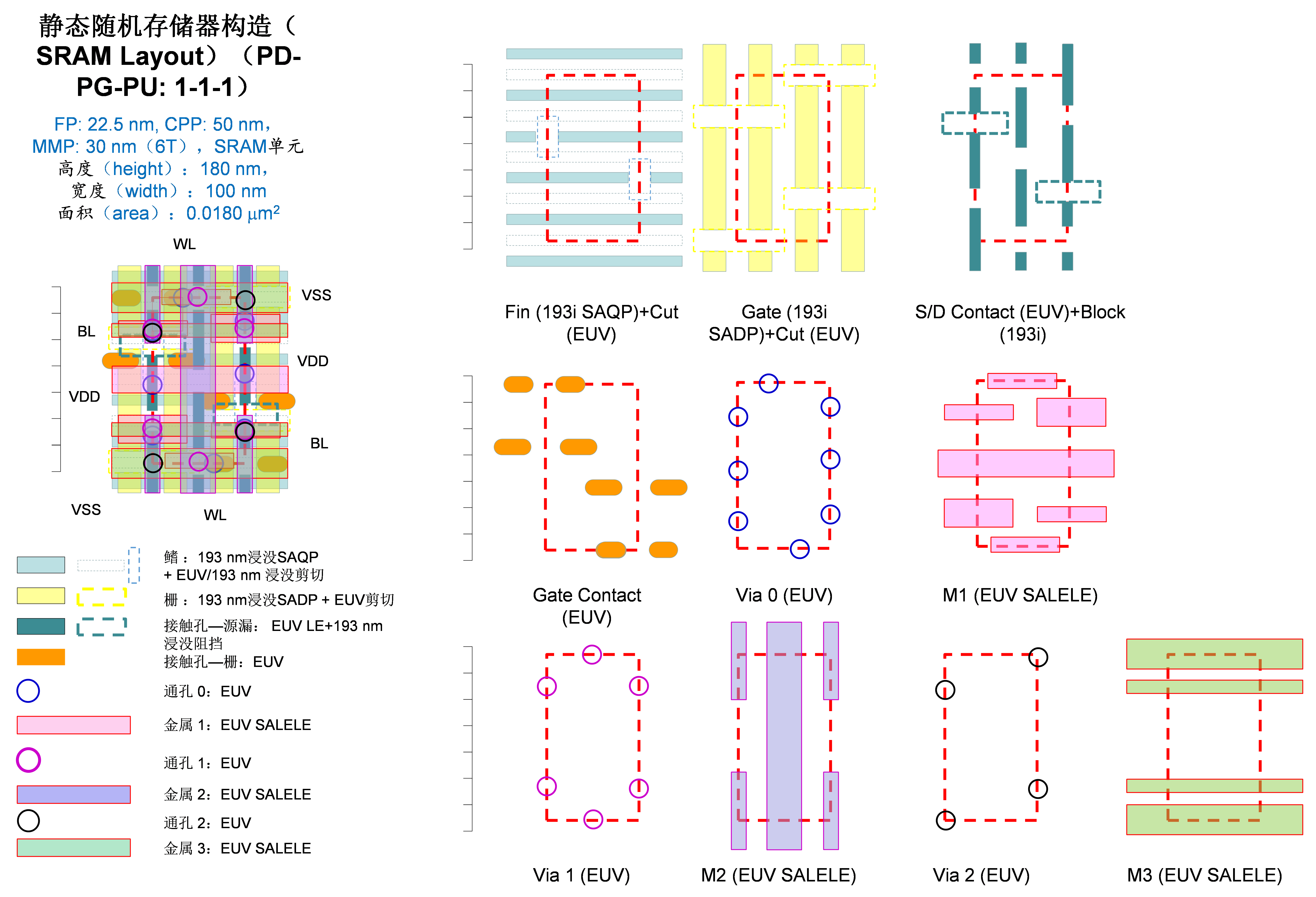
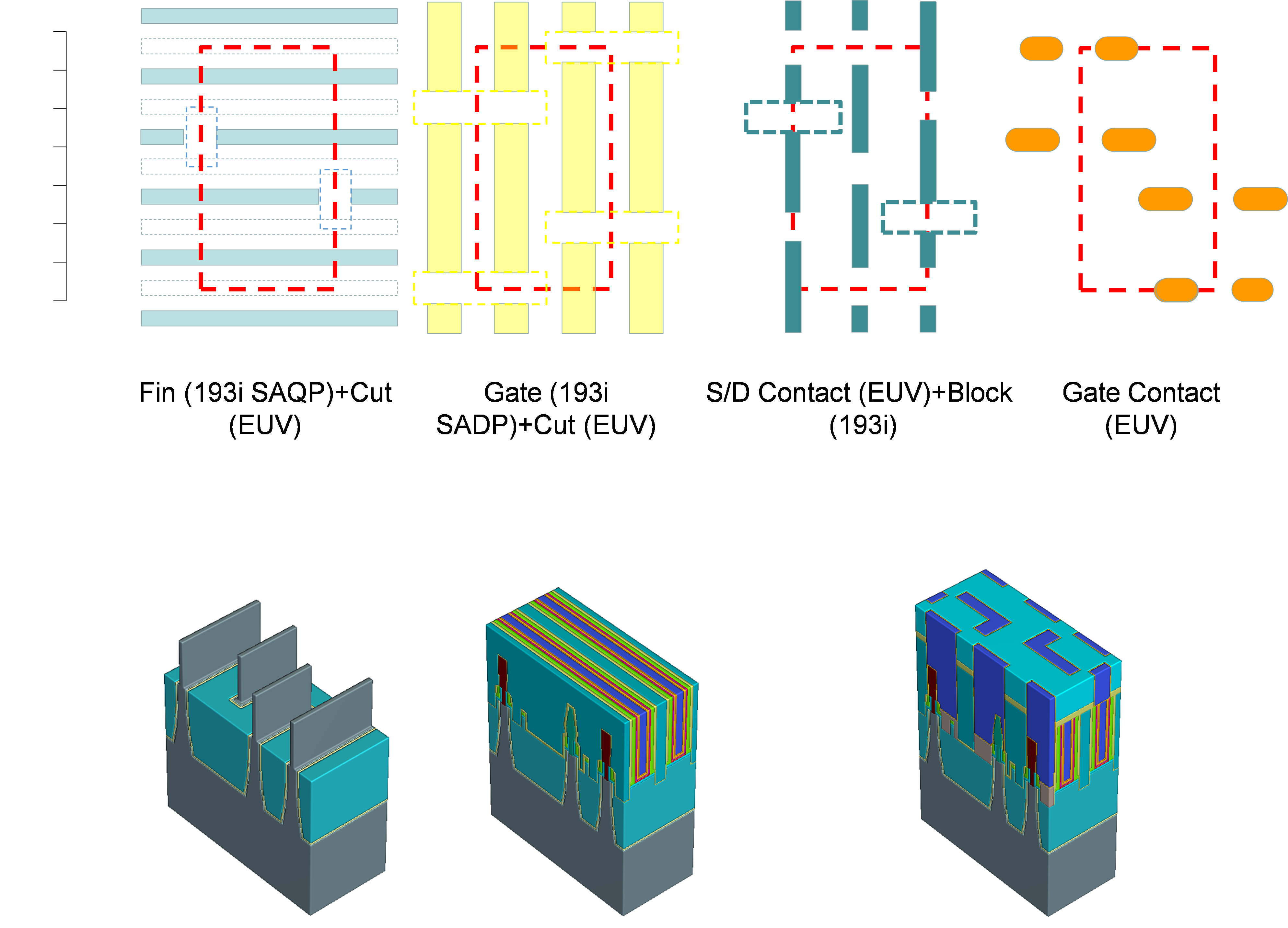
Shown in Figure 2 is a tentative Static Random Access Memory (SRAM) cell with 1 fin, respectively, for each of the PD, PG, and PU transistors, which is the densest SRAM cell. This cell poses highest challenge to the manufacturing process due to narrow space between relatively speaking tall patterns. Shown in Figure 3 is a 3D thin film model for the front-end-of-the-line (FEOL) and middle-end-of-the-line (MEOL) process of the SRAM cell built with Synopsys Sentaurus software.
Table 1.
Pitch ranges for the Fin, Contact to Poly, and Metal layers at 10 nm, 7 nm, and 5 nm logic technology nodes. | Technology Node | 10 nm | 7 nm | 5 nm |
| Fin Pitch (nm) | 33~42 | 27~30 | 22.5~25 |
| Contact to Poly Pitch (nm) | 66~68 | 54~56 | 44~50 |
| Metal Pitch (nm) | 44~48 | 36~40 | 30~32 |
Figure 2.
A tentative layout design for a PD-PG-PU 1-1-1 SRAM cell under 5 nm logic design rule. Figure 3.
A tentative FEOL and MEOL process flow for a PD-PG-PU 1-1-1 SRAM cell under 5 nm logic design rule. 3. A Strategy for the 5 nm Photolithographic Process Design
Based on the basic design rules outlined above, we choose the following photolithographic process conditions. The criteria for the choice of photolithographic process condition is based on acceptable linewidth uniformity and process window, minimized design rule restriction, minimized cost, and acceptable cycle time. Here we provide process description for 3 typical layers: Fin, Gate, and Metal.
For the Fin and Gate layer, due to very high requirement in linewidth uniformity and line edge roughness (LER)/linewidth roughness (LWR), we choose 193 nm immersion with self-aligned quadruple and double patterning methods (SAQP and SADP), respectively. This is because, any single lithographic process will produce a linewidth roughness of 4~7 nm, which is too high to satisfy a spec of 2 nm or less (according to 2017 IRDS lithography tables, the 3-sigma LER requirement for 5 nm gate layer is 1.1 nm
[1]). During SAQP or SADP, the linewidth roughness is defined by spacer thin film deposition that has theoretically near zero variation. According to a recent study, the total LWR can reduce from about 7 nm to 2 nm while LER can also be reduced to around 2 nm
[3]. In the study, the initial LWR and LER is quite high around 7 and 5 nm, respectively. Recent progress indicates that the initial numbers of LWR and LER can be reduced to 5 and 3.5 nm, respectively, which can yield a final LWR and LER both approaching 1 nm. Therefore, the SAQP or SADP is necessary for the Fin and Gate layers. Considering that 193 nm immersion lithography is both cheaper and faster (around 275 WPH for an ASML NXT2000i compared to around 60 real WPH for an ASML 0.33NA EUV tool), we choose 193 nm immersion lithography for the Fin and Gate layers. Of course, the cut layers, such as the horizontal Fin cut, the gate cut, and the single diffusion break (SDB) cut must use EUV, due to the cut width is around a fin pitch, or 22.5~25 nm, which is too difficult for 193 nm immersion lithography with high aspect ratio etch process. Shown in Table 2 is a basic design rules and recommended patterning strategy for 10 nm, 7 nm, and 5 nm process. From the table, we have found that for all 3 generations of technology, the 193 immersion SADP or SAQP has been used or recommended.
For the metal layer, since the 10 nm technology node, the metal pitch is around 44~48 nm, since it is believed that the 48 nm is the minimum pitch that can accommodate LELELE process. Due to many layers of metal lithography, the industry adopts self-aligned process as the main stream process that can reduce overlay budget. This is because, the on product overlay for the exposure tools can not satisfy the total overlay budget with multiple litho-etch and litho-etch process. The on-product-overlay (OPO) at 5 nm process is set to be 2.5 nm with matched-machine-overlay (MMO) of 2.0 nm.
Since the 5 nm is believed to be the first technology node that adopts EUV on a large scale. A total of 14 layers are believed to use EUV technology, including 3 layers of cut in the FEOL, source, drain contact and via 0 layers in the MEOL, metal layers and via X layers in the back-end-of-the-line (BEOL).
Table 2.
A strategy for the 5 nm Photolithographic process for Fin, Gate, and Metal layers. | Technology Node | 10 nm | 7 nm | 5 nm |
| | Patterning Process | | Patterning Process | | Patterning Process |
Fin Pitch
(nm) | 33~42 | 193 nm immersion SAQP,SADP | 27~30 | 193 nm immersion SAQP | 22.5~25 | 193 nm immersion SAQP |
| Contact to Poly Pitch (nm) | 66~68 | 193 nm immersion SADP | 54~56 | 193 nm immersion SADP | 44~50 | 193 nm immersion SADP |
| Metal Pitch (nm) | 44~48 | 193 nm immersion SALELE,LELELE | 36~40 | EUV/193 nm immersion
SALELE | 30~32 | EUV
SALELE |
4. Difference between EUV Lithography and DUV Lithography
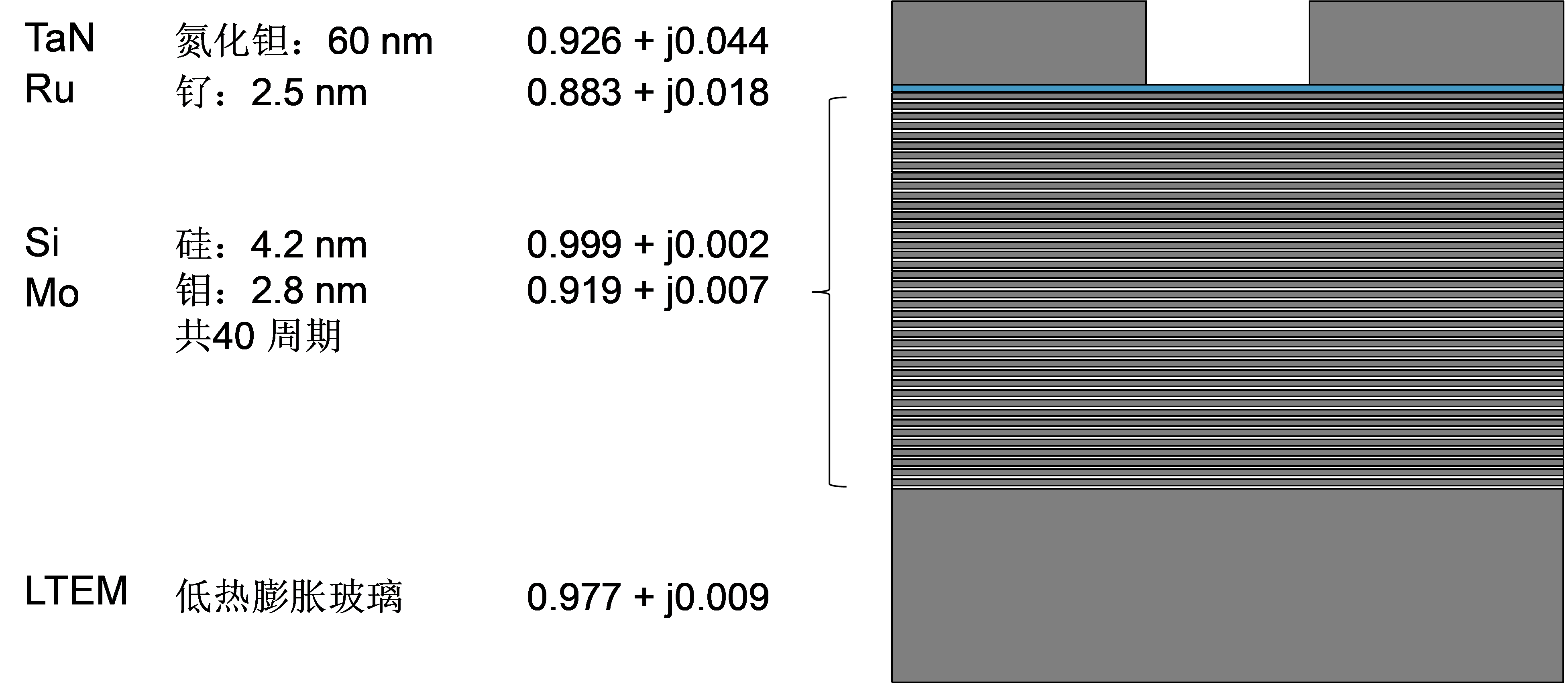
Shown in Figure 4 is the film stack that we use to do the EUV mask 3D simulation. In EUV lithography, the simulation is more tedious than that of 193 nm. In the film stack, there are not only absorption layers, but also 80 alternating high-low highly reflecting layers that located below the absorber layer. The layers consist of 40 pairs of alternating 4.2 nm silicon and 2.8 nm molybdenum materials. In order to simulate the stack, if we use finite-difference time-domain (FDTD) algorithm for the 1-dimensional pattern simulation, the maximum discretization step needs to be the common divisor of 4.2 nm and 2.8 nm, which is 1.4 nm (193 nm immersion can use 5 nm grid size, which is much larger). And due to the existence of non-zero illumination chief angle of 6°, a perfect matching layer (PML) boundary condition needs to be adopted, which automatically invalidates periodical boundary condition. It requires at least 7 periods to approximate dense patterns. Also because of reflecting imaging, the time step will need to be at least twice as long as the transmission imaging case. In addition, the amplitude from under the mask needs to subtract the incident wave amplitude to get net reflected amplitude, which will add twice as much simulation. Adding PML layer thickness and 3 incident pupil positions, the EUV simulation work load is about more than 340 times that of 193 nm simulation load. For 2D pattern simulation, the simulation load will further increase to about 1000 times due to more pupil (9 pupil locations in 2D compared to 3 in 1D) is sampled. Therefore, although in 1D, we use FDTD algorithm to do the mask modeling, in 2D, we can not use FDTD algorithm, we will take the much faster rigorous coupled wave analysis (RCWA) algorithm instead.
The RCWA method discretizes in the horizontal dimensions while stay analytical in the vertical direction. The discretization step size is connected to the number of Fourier orders that are adopted for simulation. The number of Fourier orders used is related to the length of the simulation domain. We have used 35 orders in each of X and Y dimensions.
Figure 4.
A cross section structure we use for EUV mask 3D simulation. The EUV photolithographic process differs from 193 nm immersion process mainly in the following 6 areas: the k1 factor, the shadowing effect, the horizontal-vertical (H-V) linewidth difference, the mask 3D scattering effect, the effect of photon absorption stochastics, and the aberration sensitivity.
4.1.
k1 Factor
For 193 nm, at the frequently used half pitch of 45 nm, the k1 factor is around 0.31, described in Equation (1). For EUV, if we consider a minimum half pitch of 18~20 nm, the k1 factor is around 0.44~0.48, as described by Equation (2). This indicates that the k1 factor for EUV is larger than that for 193 nm immersion and, according to experience, optical proximity effect is not significant if k1 is 0.4 or greater.

(1)

(2)
4.2.
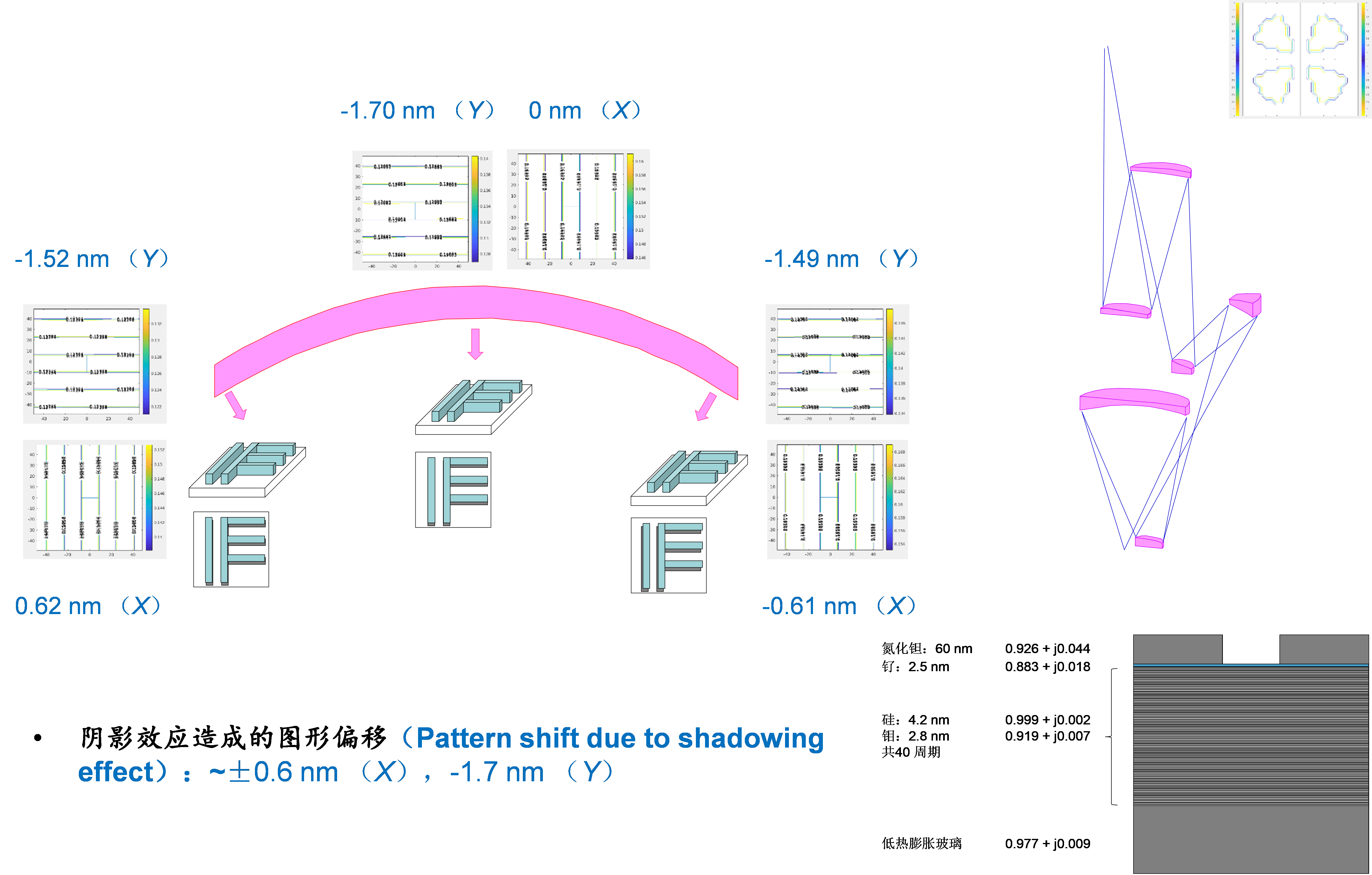
Shadowing Effect
Due to existence of non-zero chief ray angle in the illumination, the photoresist pattern may shift in the horizontal plane. As depicted by Figure 5, we have used a quasar illumination to simulate the shadowing effect in the center and left and right edges of the exposure slit and what we have found is that the slit center will witness a 1.7 nm pattern shift toward –Y direction, while at the slit edges, the –Y direction shift becomes slightly less, about 1.5 nm and there are around 0.6 nm shift in +X and –X directions, respectively, for the left and right slit edges. All these shifts are sizable compared to an overlay of 2.5 nm and needs to be corrected by optical proximity correction (OPC).
Figure 5.
Simulated EUV shadowing effect with a 32 nm pitch line and space pattern. The illumination condition is a Quasar 45° 0.9-0.2 partial coherence factor and 0.33 NA. 4.3. Horizontal-vertical (H-V) Linewidth Difference
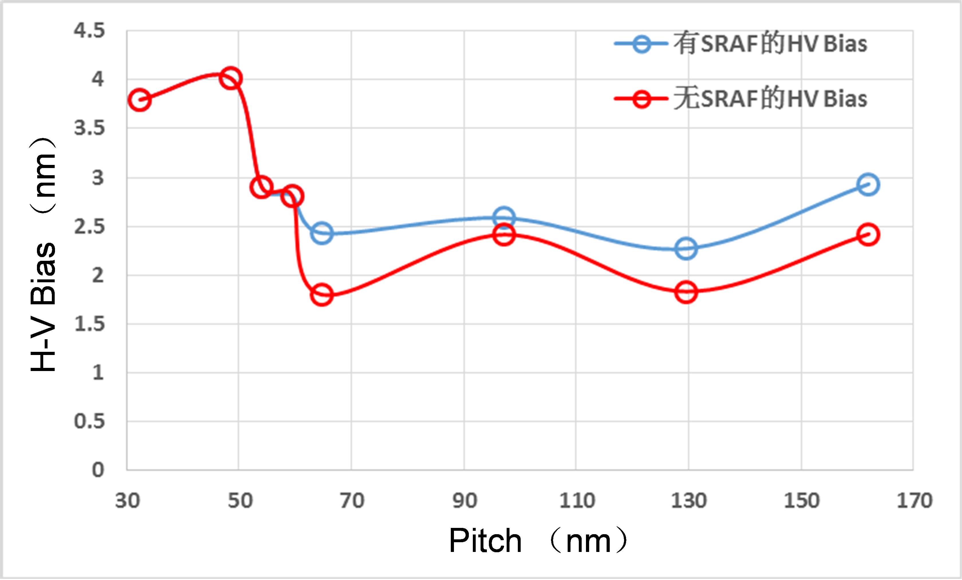
From our simulation, we have found and H-V bias (Y-direction oriented line linewidth minus X-oriented line linewidth) around 2.5~4 nm from pitch 32 nm through 162 nm, described by Figure 6.
Figure 6.
Simulated EUV H-V bias for line and space through pitch pattern. The illumination condition is a Quasar 45° 0.9-0.2 partial coherence factor and 0.33 NA. 4.4.
Mask 3D Scattering Effect
The mask 3D effect has been first considered in the process development of the logic 28 nm process, where both illumination amplitude attenuation and phase shift in the diffracted light has been found to be significant. The effect of mask 3D scattering on a 6% Attenuated Phase Shifting Mask (Att-PSM) can cause a drop of Exposure Latitude (EL) by about 20-30% and a common Depth of Focus (DoF) reduction by 25-40%, or 20~30 nm reduction. The remedy to reduce the 193 nm mask 3D effect is to introduce thinner absorption layer in the mask, or introducing the so-called Opaque Molybdenum silicide On Glass (OMOG) mask. However, at the same time of restoring the common DoF to about 85~90% and a lower Mask Error Factor (MEF), the EL is even lower than that of the 6% PSM due to the binary nature.
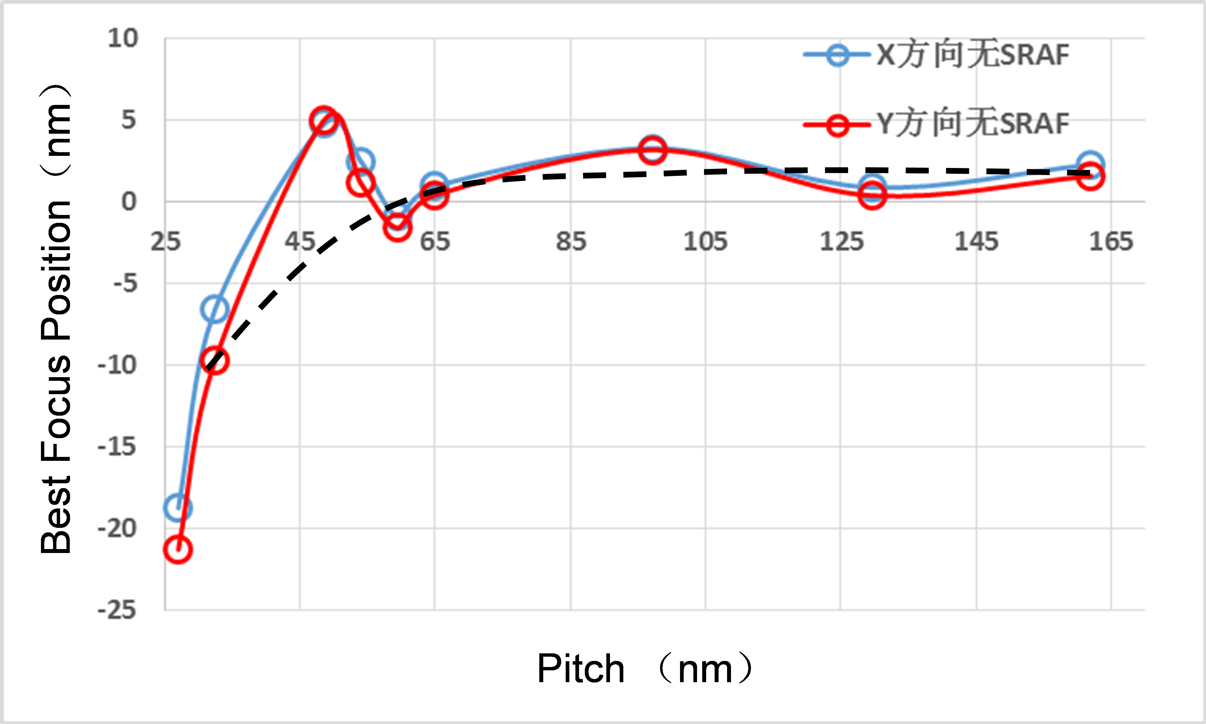
In EUV, the mask stack topography includes a tall TaN absorber, around 60 nm and a 40 alternating High-Low refractive index layer mirror, around 280 nm deep. Although the mask opening for a trench 13 nm (26 nm minimum pitch) is 52 nm (4X mask), which is much larger than the wavelength of 13.5 nm, the aspect ratio can cause significant mask 3D scattering. Shown in Figure 7 is a simulated bet focus shift as a function of pitch, indicating that the focus variation through the pitches can be as high as 25 nm in both X and Y directions. For process design, this 25 nm has to be taking into account for common DoF. Note that the reduction of common DoF by 25 nm is quite similar to that of 193 nm immersion case we just described above.
Figure 7.
Simulated EUV best focus shift for line and space through pitch pattern. The illumination condition is a Quasar 45° 0.9-0.2 partial coherence factor and 0.33 NA. 4.5.
Effect of Photon Absorption Stochastics
This effect is unique to EUV lithography. In the 193 nm immersion lithography, the photo energy is around 6.4 eV, while at 13.5 nm EUV wavelength, the photo energy is around 91.8 eV. The number of photons at any given amount of energy for the EUV is only 7% that of 193 nm immersion. Due to Poisson statistics, the fluctuation of photons scales as the square-root of their total number. The fluctuation of EUV photons is around 3.8 times that of 193 nm immersion. In 193 nm lithography, the LWR/LER is not a strong function of the exposure energy, but in EUV the LWR/LER is highly dependent on the exposure energy and scales as the inverse square-root. We have built an EUV photoresist model with stochastics. Shown in Figure 8 is simulated resist top-down profile for typical a chemically amplified photoresist (CAR), and a typical non-chemically amplified (non-CAR) metal containing photoresist. The simulation data indicate that the LWR for a typical 30 nm thick chemically amplified photoresist is about 4 nm and an EL of 15.5% at a pitch of 27 nm with dipole illumination, while for a typical metal containing photoresist, which can have 3~4 times more EUV absorption, the LWR can be better, around 3.4 nm with even lower exposure energy. Besides, the EL is significantly better than that of CAR photoresist. The non-CAR photoresists do not have photoacids as catalysts, it instead relies on photo-induced cross-linking to form negative image. For CAR photoresist at EUV, the Gaussian diffusion length is usually smaller than 5 nm, which can cause some imaging blur. For non-CAR photoresist, the photo-induced cross-link will be restricted to the size of single molecules, around 1~3 nm in diameter, which can have much higher imaging contrast.
Figure 8.
Simulated resist top-down profile for (a) a chemically amplified photoresist (CAR), and (b) a non-chemically amplified (non-CAR) metal containing photoresist. Stochastics can not only aggravate pattern edge roughness, it can also cause patterning defectivity. It has been shown that it can cause line breaking when the lines are little bit too narrow and can cause bridging when the lines are little bit too wide, as depicted in Figure 9
[4 ]. A good photolithography process needs to stay between the two defectivity limits, which means a good control on the linewidth needs to be implemented.
Figure 9.
Defect types from EUV resists after exposure and development. [4] In 2019, an IMEC study has demonstrated that the stochastics caused defectivity varies exponentially with linewidth or pitch change for both line/space and contact holes
[4], as shown in Figure 10. From this study, we can extrapolate the defectivity trend and find the minimum linewidth and pitch that can have a defectivity density level to below 10
-12 with ±7~10% total linewidth control. Although there may be other defectivity sources, such as some defectivity “floors”
[4] regardless what linewidth or pitch we use, we choose not to consider in this study. This is because either they are not limited by physics and can sooner or later be solved, or they can be fixed by following plasma etch process.
Figure 10.
Defect density as a function of linewidth and pitch. [4] From extrapolation, we found that the minimum contact hole pitch is around 48~50 nm with a 26 nm linewidth and ±2.5 nm linewidth window; the minimum line/space pitch is around 36~40 nm with a linewidth of 19 nm and ±2 nm linewidth window.
4.6.
Aberration Sensitivity
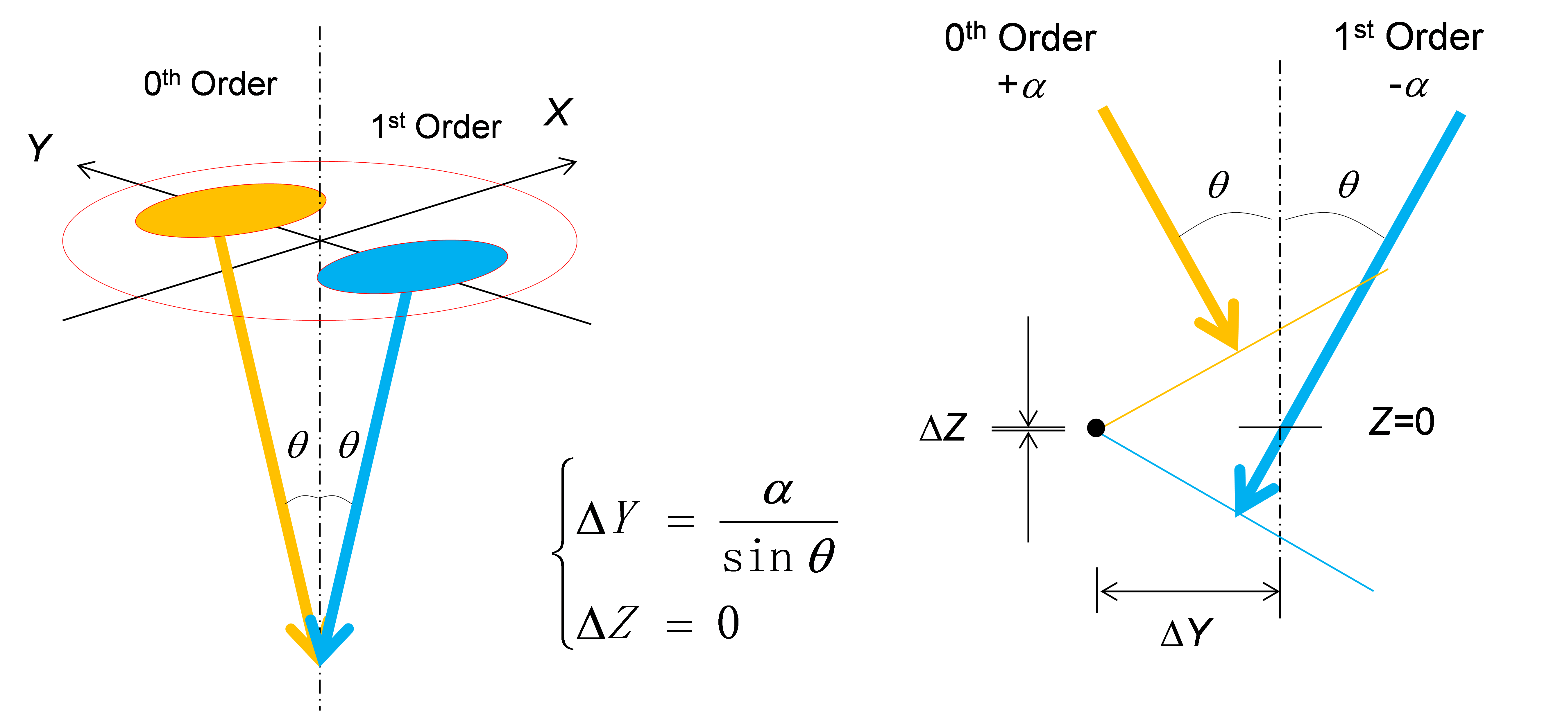
Another difference between the EUV and 193 nm immersion is the enhanced aberration sensitivity. Shown in Figure 11 is an example with coma aberration along the Y direction in the exit pupil, the coma has caused the pattern to shift in the Y direction and the shift is inversely proportional to the sine of polar angle. Since the polar angle is proportional to the Numerical Aperture (NA), the patterning sensitivity is inversely proportional to the NA. Since in 193 nm immersion lithography, the NA is 1.35 and in current EUV lithography, the NA is 0.33, the pattern shift sensitivity to aberration, e.g., coma is about 4 times more for EUV than for 193 nm immersion. In 193 nm exposure tool, we usually control the aberration to less than 1 nm (rms), therefore, in EUV exposure tool, such control has to be at least 0.25 nm (rms). Considering overlay budget and difficulties in building an EUV lens, the actual control on the aberration is around 0.18 nm (rms) for the 5 nm node.
Figure 11.
Schematic diagram of coma induced pattern shift as a function of illumination pupil position. 5. Current Capability of EUV Lithography and Its Application to the 5 nm Process Flow
With above analysis, we report our studies on the 5 nm EUV photolithography process design. As we have mentioned above, EUV are applied to FEOL and MEOL cut and contact layers and metal and via layers in the BEOL. The reason that EUV is not applied to the FEOL fin or gate layers is because the single exposure EUV LER/LWR can not compete with SADP or SAQP 193 nm immersion process. The second consideration to use EUV to do most of the cut and hole layers is because of the defectivity. The pattern density of cut of holes layers are much smaller than that of the line/space layers, usually by about an order of magnitude smaller.
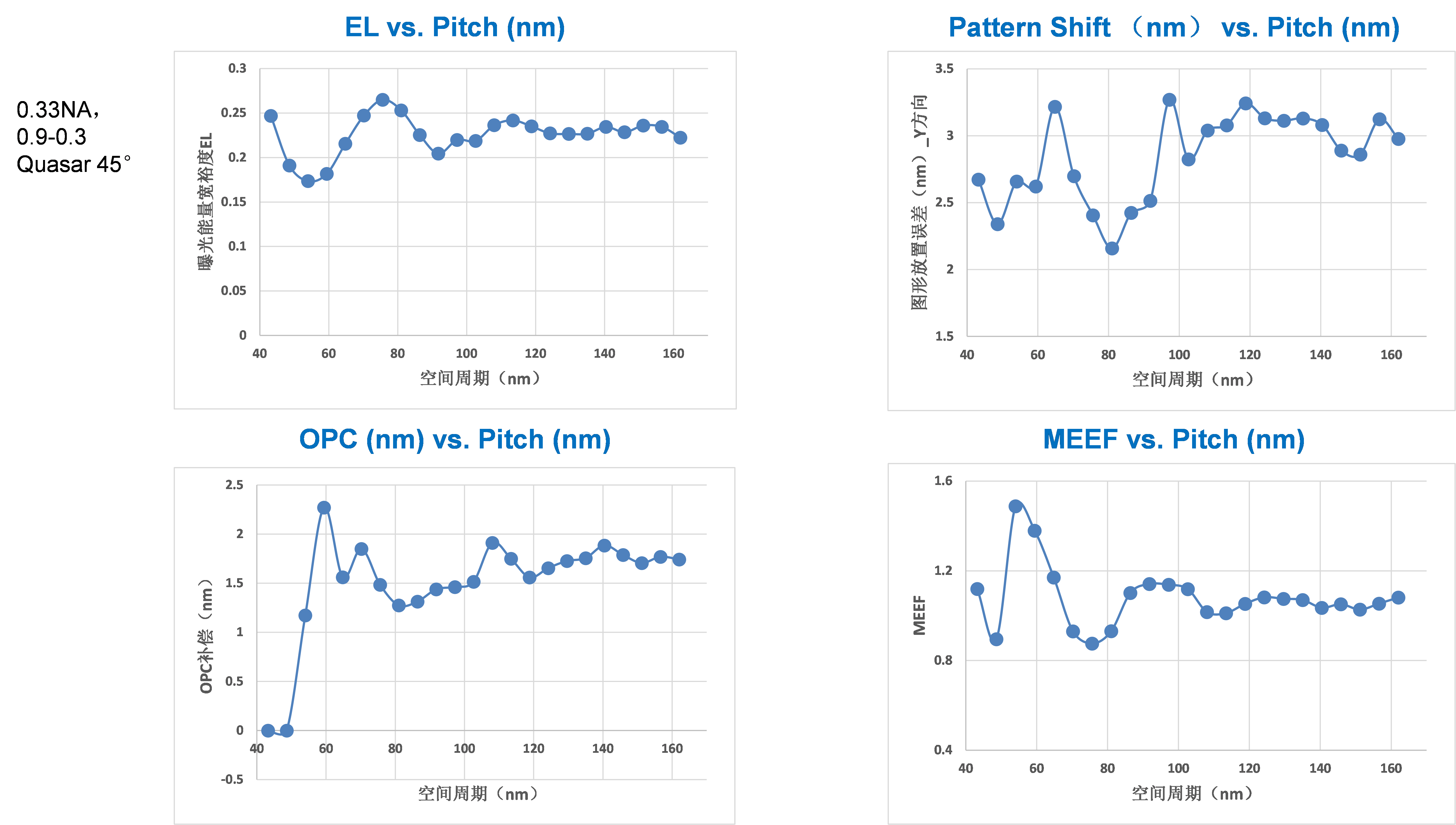
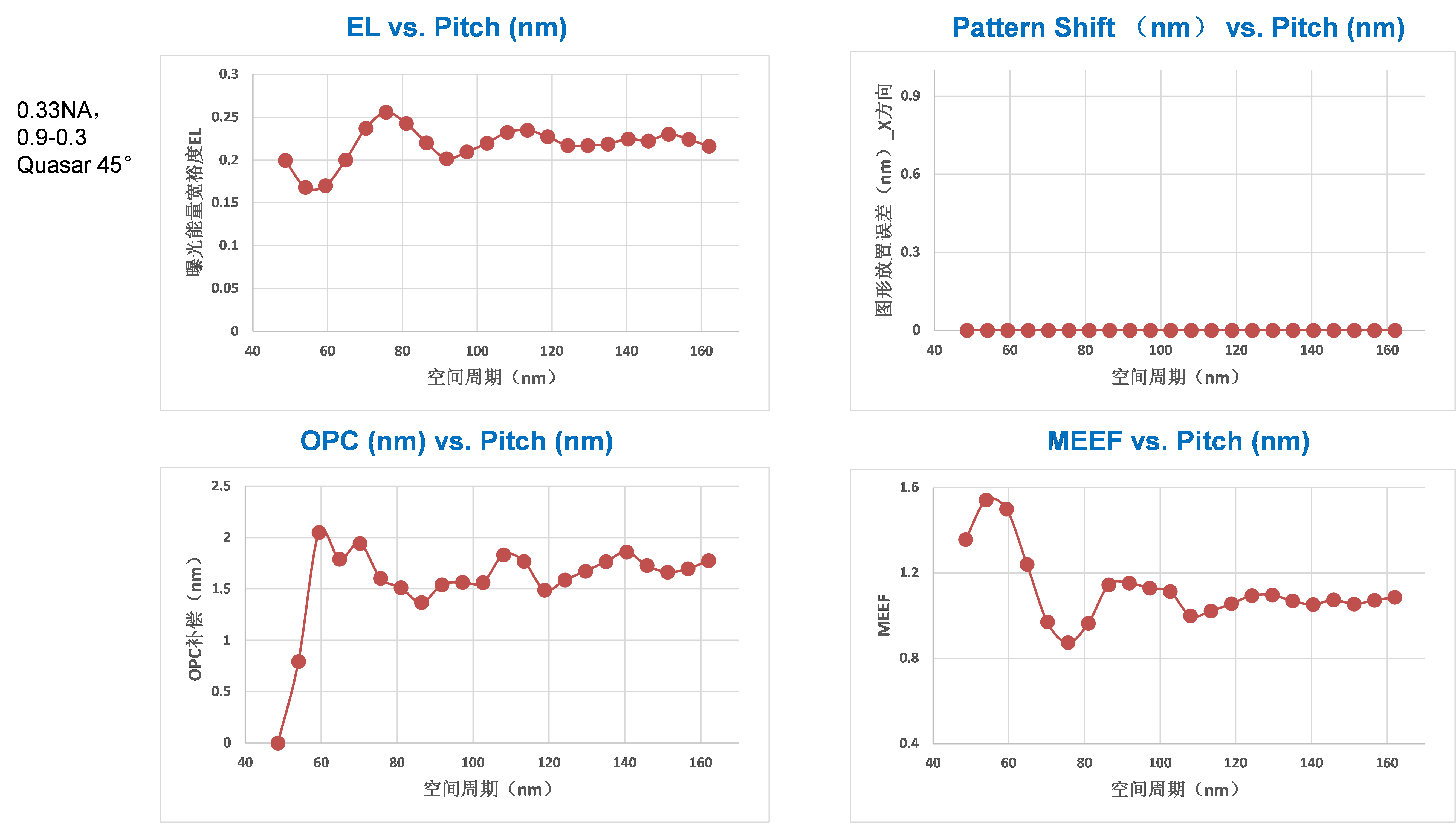
Shown in Figure 12 is a process window simulation for X-oriented 1D trench width through pitch at the slit center position. The minimum pitch we use is 43.2 nm and the trench width target is 22.5 nm. We have used a NA of 0.33 and 0.9-0.3 Quasar 45° partial coherence setting with a typical 30 nm thick chemically amplified photoresist. What we have found are: throughout all pitches, the EL is above 18%, the MEF is below 1.5, the pattern shift due to 6° chief illumination angle is around 2.1~3.3 nm toward –Y direction. The maximum optical proximity correction (OPC) is less than 2.5 nm, which is due to the minimum pitch we use is 43 nm, yielding a
k1 factor of 0.52. The simulated common DoF is more than 150 nm. As we have stated before
[5 ], for all of 0.25
m through 7 nm, the EL for the gate layer, which has the highest requirement in linewidth uniformity and roughness, has been about 18% or better and for connecting metal layer, the EL has been 13% or better. This number is obtained considering patterns under different proximity environment and all patterns need to have acceptable process window. The process window includes EL, DoF, and MEF. The EL and MEF are related to linewidth uniformity control and the DoF is related to the exposure tool performance. In EUV, due to the fact that the existence of stochastics can cause uncertainty in the pattern edges, the imaging contrast needs to be as high as possible to improve pattern edge definition. The cut layer at 5 nm design rule has a minimum pitch around 45 nm, which has a
k1 factor of 0.55 can in principle has 100% imaging contrast, or an EL around 31.4% under two beam imaging. Due to the need to maintain a practical pupil fill ratio (≥20%), DoF and MEF optimization, we use a weak Quasar and have obtained an average EL around 22.6% with minimum EL greater than 18%. Note that this level of EL is normally provided for the gate layer under 193 nm immersion lithography.
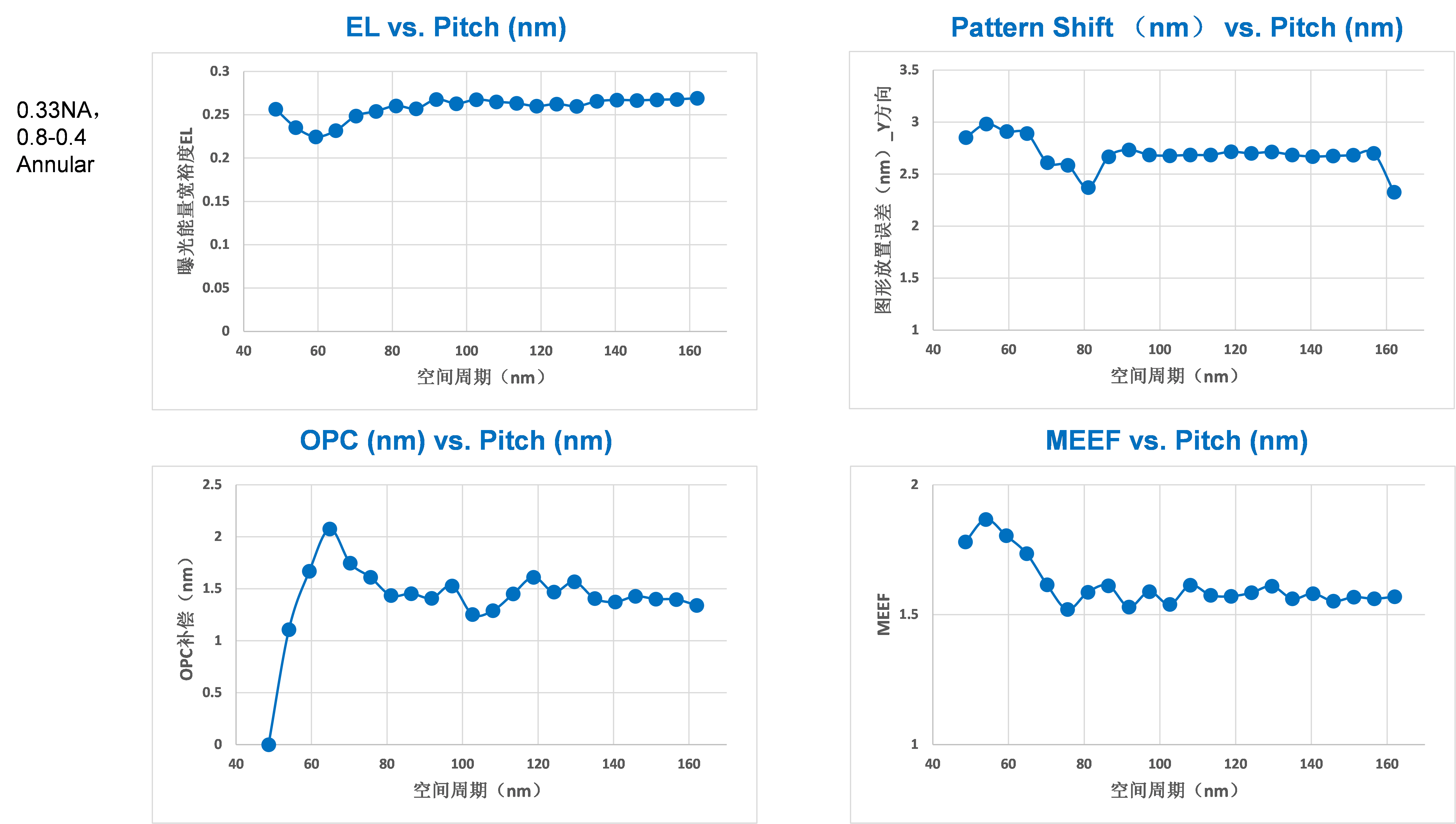
Similarly, shown in Figure 13, for cut layers oriented along the Y-axis located in the slit center. The minimum pitch we use is 48.6 nm and the trench width target is 22.5 nm. The same illumination condition will yield an average EL of 21.8% with minimum EL of 17%, a max MEF of 1.54, a maximum OPC of 2.05 nm, and a common DoF of 145.8 nm. There is no pattern shift with this orientation.
Figure 12.
Simulated lithographic process window performance on X-direction oriented 1D line/space through pitch with FDTD algorithm. Slit position: center. Figure 13.
Simulated lithographic process window performance on Y-direction oriented 1D line/space through pitch with FDTD algorithm. Slit position: center. Shown in Figure 14 is a process window simulation for 2D hole linewidth through pitch at the slit center position. We have used a NA of 0.33 and 0.8-0.4 annular partial coherence setting with a typical 30 nm thick chemically amplified photoresist. This illumination condition will yield an average EL of 25.8% with minimum EL of 22.5%, a max MEF of 1.87, a maximum OPC of 2.08 nm, and a common DoF of 101.3 nm. The minimum pitch is 48.6 nm and an ADI hole diameter target is 26 nm. Since the slit position is center, the pattern shift is toward –Y direction and the shift is around 2.3~3 nm.
Figure 14.
Simulated lithographic process window performance on 2D hole through pitch with FDTD algorithm. Slit position: center. Besides the cut layers that oriented in both X and Y directions and the hole layers discussed above, the metal layer is believed to have adopted EUV as well. Due to the choice of self-aligned LELE process on a designed minimum pitch of 30~32 nm, the minimum pitch for single exposure is 60~64 nm, which is much easier compared to the cut and hole layers. We expect an EL value approach 30% and MEF near 1.0.
From above analysis, we can conclude that the current resolution in EUV photolithography process is limited by photoresist performance, which is limited by the fluctuation in photon absorption statistics.
(1) For line and space layers, the minimum pitch with 10-12 defect density is 36~40 nm with ±2 nm linewidth window and an ADI linewidth target of 19 nm;
(2) For hole layers, the minimum pitch with 10-12 defect density is 48~50 nm with ±2.5 nm linewidth window and an ADI linewidth target of 26 nm.
For photolithographic process design, it will be weighted toward the maximization of the imaging contrast, or EL to minimize the pattern edge roughness, and uncertainty. From our simulation, at a k1 value greater than 0.5, an optimized process with all of EL, MEF, and DoF can yield an average EL over 21.8% with minimum EL over 17~18%. Further optimization in the illumination condition is possible through source-mask co-optimization (SMO) to improve the minimum EL and maximum MEF through the pitches.