Research Article Archive Versions 1 Vol 3 (1) : 20030103 2020
Download
Key Process Approach Recommendation for 5 nm Logic Process Flow with EUV Photolithography
: 2019 - 11 - 30
: 2020 - 03 - 30
4532 215 0
Abstract & Keywords
Abstract: 5 nm logic process is the current leading-edge technology which is under development in world-wide leading foundries. In a typical 5 nm logic process, the Fin pitch is 22~27 nm, the contact-poly pitch (CPP) is 48~55 nm, and the minimum metal pitch (MPP) is around 30~36 nm. Due to the fact that these pitches are much smaller than the resolution capability of 193 nm immersion lithography, it is also the first generation which adopts EUV photolithography technology on a large-scale where the process flow can be simplified by single exposure method from more than 10 layers. Relentless scaling brings big challenges to process integration and pushes each process module to the physical and material limit. Therefore, the success of process development will largely depend on careful balance the pros and cons to achieve both performance and yield targets. In the paper, we discussed the advantages and disadvantages of different process approaches for key process loops for 5 nm logic process flow, including dummy poly cut versus metal gate cut approaches in the metal gate loops, self-aligned contact (SAC) versus brutally aligned contact (BAC) approaches, and also introduced the self-aligned double patterning approach in the lower metal processes. Based on the above evaluation, we will provide a recommendation for module’s process development.
Keywords: 5 nm Logic Process; EUV; metal gate cut; SAC; BAC; self-aligned LELE
1.   Introduction
Since the CMOS technology entered nanometer era, FinFET has become the mainstream technology of device scaling. 5 nm logic process is the current leading-edge technology which is under development in world-wide leading foundries. In a typical 5 nm logic process, the Fin pitch is 22~27 nm, the contact-poly pitch (CPP) is 48~55 nm, and the minimum metal pitch (MPP) is around 30~36 nm [1]. With the continuous pattern pitch shrinking, especially into the 5 nm node, the challenge to the process becomes more and more severe. The multiple patterning technology with 193 immersion lithography become too tedious and uncontrollable since it may require 5 or 6 exposures for a single layer for 5 nm technology node. Extreme Ultra-Violet (EUV) lithography is a promising technology considered for exposure of 36 nm pitch and below. It can produce small patterns with single exposure and simplify the process flow significantly. So it is considered that 5 nm logic technology node is the first node that will adopt Extremely Ultra-Violet (EUV) lithography on a large scale.
With the application of EUV technology at the 5 nm node, the process challenges of key process loops will be changed and the traditional process approaches may not fit the new technology conditions. So we discussed the advantages and disadvantages of different process approaches for key process loops for 5 nm logic process flow, including dummy poly cut versus metal gate cut approaches in the metal gate loops, self-aligned contact (SAC) versus brutally aligned contact (BAC) approaches, and the continual use of self-aligned double patterning approach in the lower metal processes. Based on the analysis, we will provide a recommendation of process approach for 5 nm technology. All of our study is based on the 3D process simulation results with Synopsys software Sentaurus Process Explorer, and the recommendation will be a reference for the process development of 5 nm logic technology.
2.   Gate Cut Process Approach Discussion
Conventional gate cut process integration scheme is shown in Figure 1. The gate cut process is after ILD0 oxide gap filling and CMP, and before dummy poly removal process. So it is also called dummy poly cut approach. The process scheme 3D simulation is shown at the right with Sentaurus Process Explorer. From the simulation result, we can see that the major challenge of this approach is that the space between end fin and gate cut pillar is too narrow to remove the filled amorphous silicon completely and let the end fin fully covered with Work Function Metal (WFM), and this will introduce defectivity or device performance issue [2]. Since the fin and poly pitches are scaled to near 24 nm and 50 nm respectively at 5 nm node, and the cut pillar CD is about 24 nm, the space between two fins is about 43 nm, hence the space between end fin and gate cut pillar is less than 10 nm. Adding the fact that the WFM total thickness is about 6 nm for 5 nm technology, there is not enough space for two sidewall WFM coverage at all. The above analysis have not considered space variation whose 3-sigma can be 4.4 nm according to Equation (1).


Figure 1.   Dummy poly cut integration scheme and major challenge.
(1)
Because of this irreconcilable technical challenge of dummy poly cut approach, we propose metal gate cut approach for 5 nm technology which process scheme and benefit are shown in Figure 2. The gate cut process will be changed to after HKMG filling and CMP process. Because the gate cut pattern formation is after WFM filling and there is no narrow gap in dummy poly removal process, or there is no amorphous silicon residue concern. And the space between the end fin and cut pillar can be kept near 10 nm, it is enough for one sidewall WFM coverage on the end fin which thickness is about 6 nm. Even considering the space variation whose 3-sigma is about 3.6 nm with better EUV lithography overlay, the space window is enough as shown in the schematic at the Figure 2 lower right.


Figure 2.   Metal gate cut integration scheme and key benefit.
On the other hand, metal gate cut approach will bring process challenges which mainly focus on metal gate cut etch process which is described in Figure 3. Due to the complicated MG composition material, including HfO, TiN, Tantalum Nitride, TiAlC compound and W, combined with high aspect ratio (HAR) of the feature, it is hard to etch all of the materials with the same etch rate and obtain the vertical cut trench profile[3]. But essentially the process challenges can be overcome by improving etch capability with advanced ICP or ECR etcher tool and reducing HAR of the feature by new process approach such as brutal aligned contact process approach which will be mentioned later.


Figure 3.   Process challenge of metal gate cut etch.
3.   Contact Process Approach Discussion
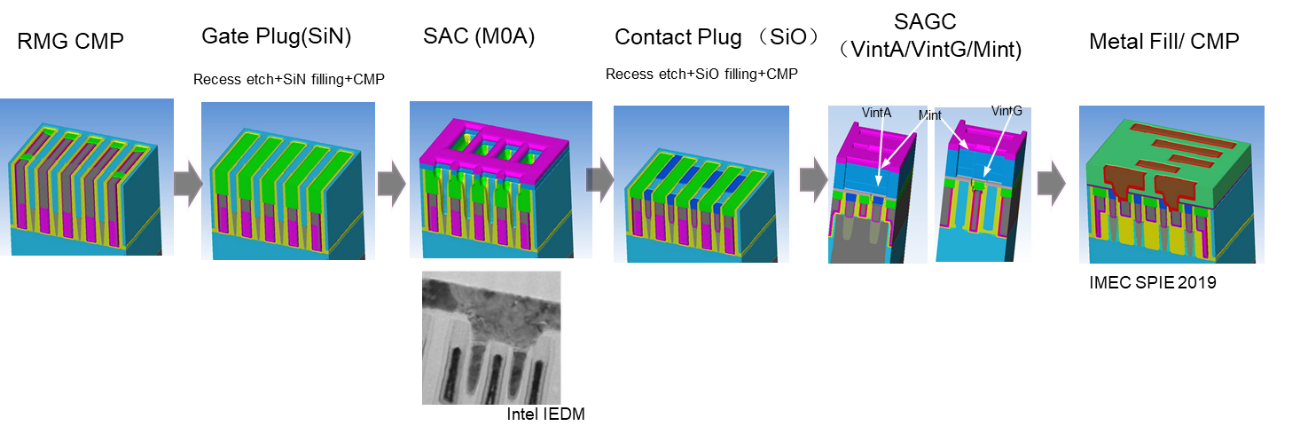
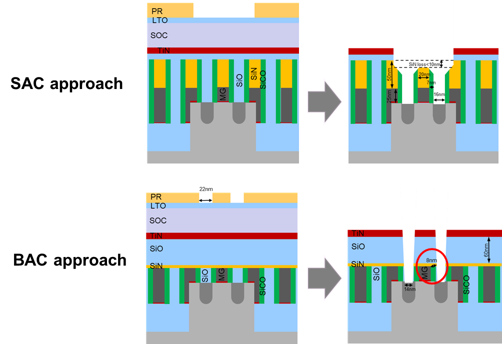
In order to reduce lithography process challenge, i.e., overlay window can be enlarged significantly by using the oversized contact mask, Self-aligned contact (SAC) approach is widely adopted to realize complex contact pattern. Figure 4 is the MOL contact patterning process flow schematics with SAC approach which is cited from IMEC SPIE paper [4]. In this process integration, the first step is to form the source/drain contact with SAC oxide etch which needs high etch selectivity to the gate plug (GP) (Si3N4) and the sidewall spacer (SiCO). The second step is called self-aligned gate contact (SAGC) which needs two separate SAC etch to form contact holes (VintG) connecting the first metal (Mint) to the gate and contact holes ( VintA) connecting Mint to source/drain contact respectively. Both of the SAC etch processes also need high selectivity.


Figure 4.   
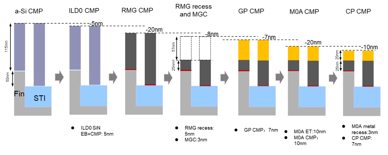
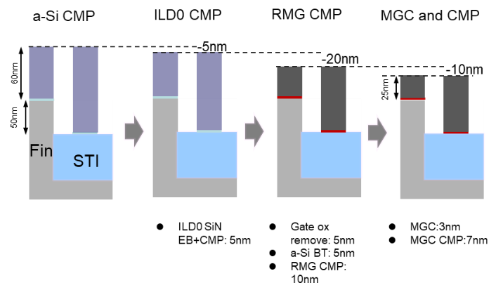
MOL contact process flow schematics with SAC approach.
SAC approach is used to shift patterning challenge from lithography to dry etch process with high etch selectivity. It is an important booster for device scaling with 193 nm immersion lithography. But the process flow is very complicated including repetitive recess etch, plug materials filling (Si3N4 for gate plug, SiO2 for contact plug) and CMP steps. The challenge of process quality control will be very large such as film thickness uniformity. Furthermore, all of these processes will consume the gate height step by step, and eventually lead to the initial gate height will be very high. Figure 5 shows gate height loss assumptions with SAC approach. The initial gate height will be about 165 nm on STI, considering the Si3N4 and SiO2 hard-mask thickness atop the α-Si before gate etch, the actual HAR will reach 9 with 32 nm gate space. This will aggravate process difficulty for subsequent etch and gap fill processes from dummy poly gate patterning.
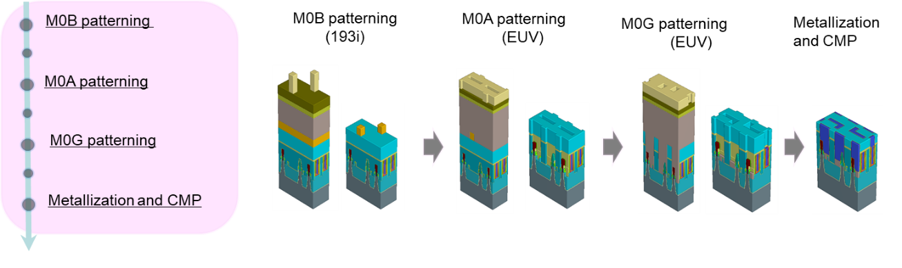
With EUV lithography, brutal-aligned-contact (BAC) can be realized for 5 nm node technology. According to 5 nm design rule, the contact pitch is about 50 nm and minimal trench CD (critical dimension) is 14 nm. 3 lithography exposures are required to realize the contact pattern, two is for the S/D contact patterning (one 193 nm immersion lithography for the S/D contact block (M0B), one EUV lithography for the S/D contact final patterning), and one is for the gate contact patterning. The BAC approach process flow is shown in Figure 6.
From the BAC process flow schematics, we can see the process is simplified with fewer process steps. It will help to reduce process variation and enhance process control. The gate height loss assumptions with BAC approach is shown in Figure 7. The initial gate height will be reduced to about 110 nm on STI, and the HAR is ~6.5 when the gate space is 32 nm including Si3N4 and SiO2 HM before gate etch. The HAR is reduced by nearly 30% compared to the previous SAC approach.


Figure 5.   Gate height loss assumptions with SAC approach.


Figure 6.   Brutal-Aligned-Contact (BAC) approach.


Figure 7.   Gate height loss assumptions with BAC approach.
For contact process, the isolation space thickness variation between contact and gate is the key parameter related to the failure of devices. We also checked the EPE (Edge placement error) window which schematics is shown in Figure 8. For SAC approach, there is no EPE window concern because the S/D contact trench position is defined by self-aligned process, and high selectivity etch ensure the isolation spacer loss is very low. But for BAC approach, the process weak point is at the top of isolation spacer, the isolation space is about 8 nm and the isolation space variation 3-sigma is about 3.5 nm with stringent process control (major specifications as: EUV overlay≤2.5 nm, LER≤1.5 nm). Under this condition, the minimal safe dielectric isolation space 4 nm can be guaranteed.


Figure 8.   Isolation space EPE window check SAC & BAC.
4.   Metal Process Approach Discussion
Metal process will continue to adopt self-aligned litho-etch-litho-etch (LELE) process with EUV lithography due to the needs for good overlay (≤2.5 nm) under ever-tightened design rules (CD~15-16 nm) [5, 6]. Figure 9 is the process flow schematics. The first step is area A patterning with EUV lithography on amorphous silicon to form the pattern with 64nm pitch CD, 48nm trench CD. The second step is TiO ALD spacer deposition which film thickness is 16nm. The third step is to form area A block pattern with 193i lithography on underlying Si3N4 layer. The fourth step is to do area B patterning with EUV lithography. Finally transfer pattern to underlying TiN hard mask layer.
The benefit of the approach is film stack and process flow are simplified, line and trench CD can be adjusted by different pitch size. With self-aligned approach, the overlay window of 2nd LE process is enlarged for area B patterning. But it needs at least 3 exposures to realize the patterning, and we invented a novel process approach with only 2 EUV exposures. The patent application is ongoing.


Figure 9.   SA-LELE lower metal patterning approach with EUV lithography.
5.   Conclusion
We have done an initial study on the key process loops for 5 nm logic process flow with EUV lithography, according to typical design rules. Gate cut process: metal gate cut approach with EUV lithography will benefit the end fin WFM coverage. Contact patterning: BAC approach simplify the process flow and reduce gate height and HAR significantly, but the processes need more stringent control due to marginal EPE window (major factors EUV overlay≤2.5 nm, LER≤1.5 nm). Backend lower metal patterning: the SA-LELE approach simplify the film stack and process flow. The 2nd LE overlay window is enlarged due to self-aligned process.
Acknowledgments
I thank the higher management team from Shanghai IC R&D Company for the support of this work.
[1] Qiang Wu, Yanli Li, Yushu Yang, Yuhang Zhao, “A Photolithography Process Design for 5 nm Logic Process Flow”, accepted by Journal of Microelectronic Manufacturing 2020, in press.
[2] Andrew Greene, Huimei Zhou, Ruilong Xie, et al, “Gate-Cut-Last in RMG to Enable Gate Extension Scaling and Parasitic Capacitance Reduction”, Symp VLSI Tech., p.144, 2019
[3] Keisuke Nakamura, Tomohiro Kitagawa1, Kazushi Osari, et al, “Plasma etching of high-k and metal gate materials”, Vacuum 80 (2006) 761–767
[4] Dunja Radisic, Marc Demand, Shihsheng Chan, et al, “Plasma etch selectivity study and material screening for Self-Aligned Gate Contact (SAGC)”, Proc.of SPIE Vol. 10963, 109630P,2019
[5] Frédéric Lazzarino , Nihar Mohanty , Yannick Feurprier, et al, “Self-aligned block technology: a step towards further scaling”, Proc. of SPIE Vol. 10149 1014908-1,2017
[6] Joost Bekaert*a, Paolo Di Lorenzoa, Ming Maoa, et al, “SAQP & EUV block patterning of BEOL metal layers on imec’s iN7 platform”, Proc. of SPIE Vol. 10143 101430H-1,2017.
Article and author information
Yushu Yang
yangyushu@icrd.com.cn
Yanli Li
Qiang Wu
Jianjun Zhu
Shoumian Chen
Publication records
Published: March 30, 2020 (Versions1
References
Journal of Microelectronic Manufacturing