Authors: Kun Yu, Hua Wang
Institution:Sino IC Technology Co, ., Ltd, ., Shanghai
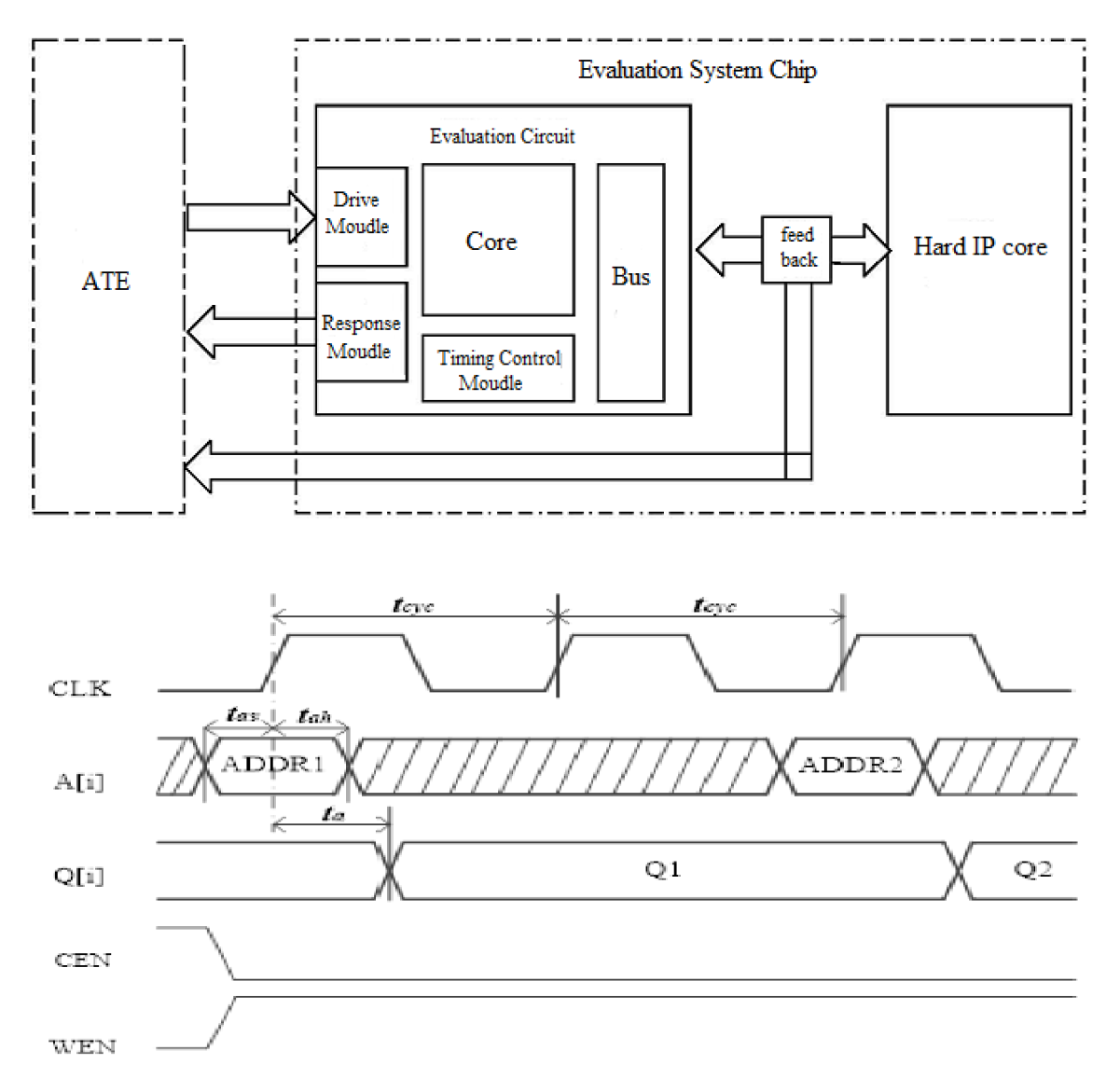
Keywords:hard IP core;system on chip (SOC);testing technology;evaluation circuit;memory;automatic test equipment (ATE)
doi:10.33079/jomm.19020201
Abstract:
Based on the analysis of the existing hard IP core testing technology, the hard IP core nondestructive testing technology was studied, according to the verification requirements of a large number o...
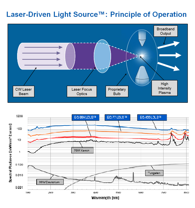
Authors: Huiling Zhu, Paul Blackborow
Institution:Energetiq Technology, Inc, ., 7, Constitution Way, Woburn
Keywords:laser-driven;brightness;broadband;deep-UV;metrology;LDLS
doi:10.33079/jomm.19020104
Abstract:
Laser-driven light sources (LDLS) have ultrahigh-brightness and broad wavelength range. They are ideal radiation sources for optical metrology tools for advanced process control in semiconductor ma...
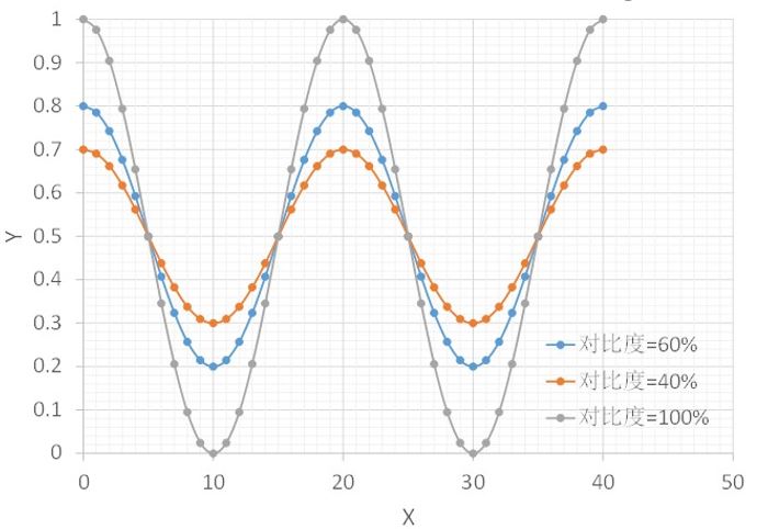
Authors: Qiang Wu
Institution:Shanghai IC R, &, D Center, Shanghai
Keywords:image projection photolithography;imaging contrast;exposure latitude;mask error factor;linewidth uniformity;chemically amplified photoresist;phase shifting mask;optical proximity correction;and photoacid diffusion length
doi:10.33079/jomm.19020101
Abstract:
Photolithography has been a major enabler for the continuous shrink of the semiconductor manufacturing design rules. Throughout the years of the development of the photolithography, many new techno...
Authors: Xingyu Zhou, Youling Yu
Institution:Tongji University, Shanghai
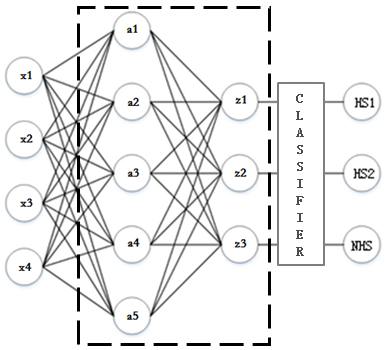
Keywords:lithography;hotspot detection;CNN;deep learning
doi:10.33079/jomm.18010205
Abstract:
In the advanced semiconductor lithography manufacturing process, the sub-wavelength lithography gap may cause lithographic error and the difference between the wafer pattern and mask pattern which ...
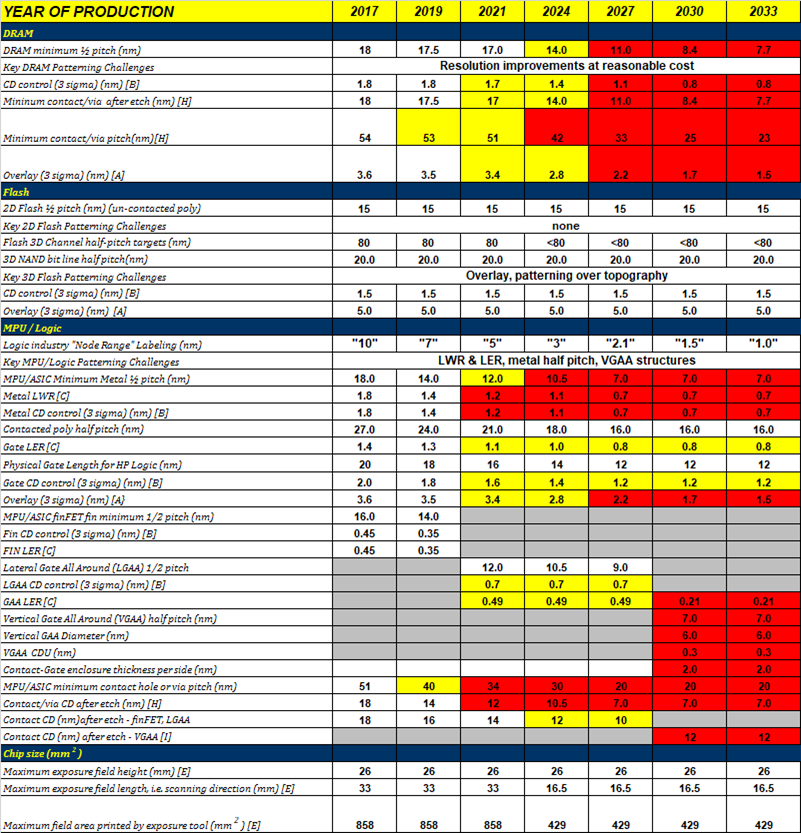
Authors: Mark Neisser
Institution:Kempur Microelectronics, Beijing
Keywords:lithography roadmap;IRDS;advanced patterning;EUV lithography;directed self-assembly (DSA);Ebeam direct write;Nanoimprint
doi:10.33079/jomm.18010204
Abstract:
Technology roadmaps have been a part of the semiconductor industry for many years. The first roadmap was Moore’s law, which started as an empirical observation that competitive forces then turned i...
Authors: Yijiang Shen, Zhenrong Zhang
Institution:Guangdong University of Technology
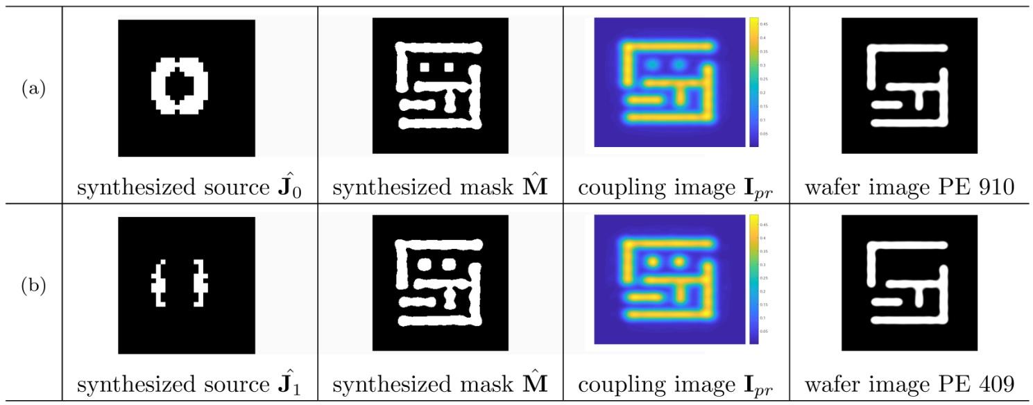
Keywords:computational lithography;variational level set;source and mask optimization;coupling image
doi:10.33079/jomm.18010203
Abstract:
This paper addresses the contributing factors in lithographic source and mask optimization, namely, the accuracy of the image formation model and the efficiency of the inverse imaging calculations ...
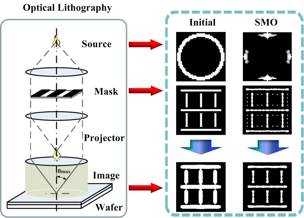
Authors: Xu Ma, Zhiqiang Wang, Gonzalo R. Arce
Institution:Key Laboratory of Photoelectronic Imaging Technology and System of Ministry of Education of China, School of Optics and Photonics, Beijing Institute of Technology, China
Keywords:Computational lithography;source mask optimization (SMO);compressive sensing (CS);inverse problem
doi:10.33079/jomm.18010202
Abstract:
Source and mask joint optimization (SMO) is a widely used computational lithography method for state-of-the-art optical lithography process to improve the yield of semiconductor wafers. Nowadays, c...
Authors: Man Zhang, Qiling Deng, Hui Pang et al.
Institution:Institute of Optics and Electronics, Chinese Academy of Sciences
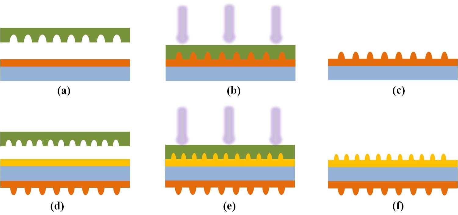
Keywords:Double-sided nanostructure, elastic substrate, soft-nanoimprinting lithography, metal layer.
doi:10.33079/jomm.18010201
Abstract:
Double-sided nanostructure has more excellent properties in high efficiency, high yield, and high capability devices, which becomes the attention spots in nanofabrication technology. We proposed a ...
Authors: Lithotechsolutions.org
doi:10.33079/jomm.18010105
Abstract:
China's IC industry has been flourishing in recent years, huge market demand together with government investments are the major driving forces for this development. The status and development momen...