Research Article Archive Versions 2 Vol 2 (2) : 19020201 2019
Download
Hard IP Core Nondestructive Testing Technology
: 2019 - 05 - 10
: 2019 - 06 - 10
2028 29 0
Abstract & Keywords
Abstract: Based on the analysis of the existing hard IP core testing technology, the hard IP core nondestructive testing technology was studied, according to the verification requirements of a large number of hard IP core precise and fast testing. Combined with the external automatic test equipment(ATE)and the on-chip evaluation circuit, a general evaluation system of simulating user system on chip (SOC) with signal timing calibration and compensation by software and hardware compensation structures were introduced to realize the function, performance and reliability verification of the hard IP core. The design and verification of a random access memory (SRAM) hard IP core based on an on-chip evaluation circuit was actually completed, and the key timing parameters of the hard IP core were tested. The address setup time parameter was taken as an example to analyze the specific testing method and the test results were obtained. With this testing technology, the accuracy of testing the timing parameters of hard IP core can reach pS level, compared with the hard IP core packaged test, the accuracy of the result data is fully reflected.
Keywords: hard IP core; system on chip (SOC); testing technology; evaluation circuit; memory; automatic test equipment (ATE)
1.   Introduction
As the scale of integrated circuit (IC)increases, more and more system on chip (SOC) integrate various IP cores (also known as Know Good Die, KGD) which have been tested and verified, such as CPU, AD/DA, memory, interface and so on, to achieve powerful and complex functions. IP cores are the key to the success of SOC design [1-2]. According to statistics, the cost of testing and verification of the SOC and various IP cores has exceeded 50% of the design cost and increased by about 10.5% every year. Moreover, the test and verification time of SOC and IP cores has greatly exceeded the design time [3]. The testing and verification of SOC and IP core has become the bottleneck of SOC technology development. Based on the advanced semiconductor process and materials, the performance and complexity of IP core are constantly increasing, which leads to the new types of defects. New fault models and new test algorithms must be adopted to detect them. The response of IP core is compared with the expected response by applying excitation to the input of IP core, and its function and timing errors can be found. Thus, by modifying the IP core, the quality and reliability of IP core can be improved [4]. The key test methods of the IP core, advanced test technologies of IP core, fast and accurate IP core test and verification are the current research hotspots.
By designing a general evaluation system of simulating user system on chip (SOC), the tested hard IP core was embedded in the test circuit. The software and hardware compensation structures were introduced to calibrate and compensate the signal timing, which could control and monitor the input signal of hard IP core accurately. Combined with the external automatic test equipment (ATE) and the on-chip evaluation circuit, the function, performance and reliability of the hard IP core test and verification could be realized. The general evaluation system chip can also be regarded as a simulated SOC environment. At the same time, the applicability of hard IP core in SOC environment was verified, and its reusability was evaluated [5].
2.   Hard IP Core Testing Technology
As the embedded SOC design based on reusable IP core becomes the mainstream of IC design, the performance of IP core determines the performance of the whole SOC. Usually, the test of hard IP core is carried out by ATE after packaging, which is similar to product test. Because bonding pad, bonding wire, packaging stress and material have superimposed effects on the test of hard IP core itself, such test results can not accurately characterize the performance of hard IP core. In wafer-level testing, most hard IP cores have been embedded in SOC. Many tests are based on built-in self-test (BIST). However, some problems of BIST itself, such as low test coverage, high test power consumption and long test time, need to be solved urgently [6], traditional design for testability of static logic structure is not enough.
Aiming at these problems, this paper mainly studies the solution of non-destructive testing for hard IP core. Combined with the external automatic test equipment (ATE) and the on-chip evaluation circuit, a general evaluation system of simulating user system on chip (SOC) with signal timing calibration and compensation by software and hardware compensation structures were introduced to realize the function, performance and reliability verification of the hard IP core. It avoids the defect error caused by the traditional final test after packaging, and can guarantee the rationality and validity of hard IP core test results.
3.   On-Chip Evaluation Circuit Design
By designing a general evaluation system of simulating user system on chip (SOC), the complex hard IP core is embedded in the test circuit through the standard interface. This general evaluation system can be used to test many kinds of hard IP cores, such as on-chip memory, bus control, peripherals, general protocol interface and so on. The input module of the general on-chip evaluation circuit mainly converts the instructions and data from the drive module into the specific interface timing input to the hard IP core under test; the output module mainly extracts, converts, processes or directly compares the signals of hard IP core tested by ATE; because the on-chip test circuit itself will introduce delay in timing, the observation points are added between the on-chip evaluation circuit and the hard IP core to compensate the timing of the signal and realize the accurate input controlling and monitoring of the hard IP core, so as to test and verify the function and performance of the hard IP core accurately. The functional block diagram of hard IP core evaluation system is shown in Figure 1.


Figure 1.   The functional block diagram of the hard IP core assessment system.
In order to realize the accurate evaluation of hard IP core to be tested, the correctness, accuracy and reliability of the evaluation circuit itself should be guaranteed first. On-chip evaluation circuit design conforms to IEEE1500 and IEEE1149.X protocols [7-8]. Firstly, DFT testability design can be used for self-diagnosis and verification, including BIST, scanning test, etc. And in recent years, the application of advanced testing technologies is gradually improving the testing efficiency of DFT [9]. Secondly, the evaluation circuit is connected to the ATE through the load board, and it can be tested by the ATE or other instruments, including the functional protocols and electrical parameters, so as to ensure the reliability of the evaluation circuit. The key of on-chip evaluation circuit is to test hard IP core in chip as much as possible without increasing the circuit and area of hard IP core itself. It includes excitation signal generation, timing control, test vector configuration, drive circuit and control bus and other functional modules. It uses flexible and configurable standard interface to connect with hard IP core, and the hard IP core can be tested by different test cases. Because the hard IP core to be tested is embedded in the evaluation system chip, there is no interference and signal attenuation caused by wire bonding or probe impedance, so the IP can be tested at full speed to achieve accurate evaluation.
The hard IP core can be tested and verified by ATE from two aspects. On the one hand, it combines the evaluation circuit embedded in the system chip with the external ATE test environment, corrects the test deviation caused by the impedance matching, time delay and parasitic parameters of the test circuit, and compensates the uncertainty of the measurement results caused by the changes of process, voltage, temperature, impedance and noise of the evaluation circuit, which can be accurately measured through the error compensation circuit. On the other hand, ATE can directly observe the performance difference of hard IP core caused by different process. By scanning timing sequence and voltage, we can get the characterization map of the performance of the hard IP core, which is mainly used to evaluate the curve of excitation parameters and the function and response parameters of the hard IP core. The map includes single-parameter response (two-dimensional) curves, such as (power supply voltage-speed), (voltage-power consumption), two-parameter response (three-dimensional) curves, such as (power supply voltage, input voltage level) - (speed), (power supply voltage, input voltage level) - (power consumption), multi-parameter response (multi-dimensional) curves, such as (power supply voltage, input voltage level, timing) - (speed), (power supply voltage, input voltage level, timing) - (power consumption). It can be realized by shmoo test and algorithm search test. And also, process and thermal factors both have the impact on the hard IP core [10]. Figure 2 shows the maximum rate curves of 100 SRAM hard IP core at different processes, temperatures and voltages. TT/NT/NV represents the rate curves at TT process, 25 Centigrade and 1.05V of power supply voltage, SS/HT/LV represents the rate curves at SS process, 125 Centigrade and 1.155V of power supply voltage, and FF/LT/HV represents the rate curve at the FF process, -40 Centigrade and 0.945V of power supply voltage.


Figure 2.   Maximum rate curves for different processes / temperatures / voltages.
4.   Hard IP Core Test and Verification
Taking memory hard IP core as an example, this paper studies the test technology based on test evaluation circuit. Considering the timing constraints of the chip, the design methods for the universality and reusability of the hard IP core are studied. At the same time, based on the hard IP core test and verification environment, the control constraints and boundary conditions of hard IP core are obtained, and the test and verification of hard IP core function and performance are actually evaluated.
4.1. Memory Hard IP Core Function and Performance Testing and Verification
As embedded SOC design based on reusable memory hard IP core gradually becomes the mainstream of IC design, the area of memory hard IP core in SOC is increasing. Usually, the test method of memory hard IP core analyzes its physical fault defects according to its structural, transform the physical fault defects into logical faults, and use fixed logical fault model to analyze these defects. At present, the functional fault models mainly include following categories [11]: stuck at fault (SAF), stuck open fault (SOF), transition fault (TF), coupling fault (CF) and address fault (AF). Stuck faults can be divided into faults with memory cells stuck at 1 or 0.
According to different fault models, some specific states are selected, and the test information of these states are compiled into a test algorithm. The selection of memory chip test algorithm is determined by the coverage of the fault model [12-13]. That is, an effective test algorithm covering the fault model which proves whether the memory unit can erase, read and write normally is need to choose to test this memory chip. At present, the commonly used test algorithms include [14]: all "0" and all "1", Checkerboard, Gallop, March, Walk, Masest, Movi, etc.
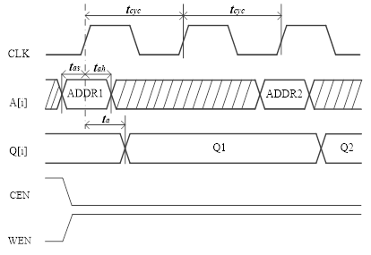
In addition to the functional testing of memory hard IP core, it is also necessary to test its timing performance. The performance characteristic parameters of memory hard IP core generally need to be tested include read and write timing, such as clock cycle (tcyc), address setup time (tas), address hold time (tah), etc. As shown in Figure 3, is a SRAM timing diagram, in which CLK is a clock signal, A is an address signal, and Q is a data output signal, CEN is chip enable signal, WEN is the write enable signal.


Figure 3.   Memory timing diagram.
4.2. Hard IP Core Test and Verification Based on On-Chip Evaluation Circuit
In this paper, two SRAM hard IP core testing based on the general evaluation system is completed to meet the requirement of hard IP core performance test. The input data setup time, address and control signal setup time, input data hold time, address and control signal hold time of SRAM hard IP core are tested by ATE and the customized evaluation system. The ring oscillator module, frequency dividing module and self-calibration module are also tested.
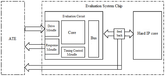
Two SRAM hard IP core chips are designed at the same time. Chip A is a normal SRAM hard IP core chip. The input and output of SRAM hard IP core are connected with corresponding driving circuits. Chip B contains a general evaluation circuit, which is mainly including three parts: the programmable master behavior simulation unit, the configurable on-chip interface module and the configurable output timing detection module. At the same time, it integrates the target tested SRAM hard IP core, the test I/O group and other clock circuits to form a standardized on-chip hard IP core evaluation circuit system. The programmable master control behavior simulation unit is the key part of the system. By applying reasonable external control incentives and internal simulation control procedures, it can perform read-write and other actions to the SRAM hare IP core, and collect corresponding feedback signals based on the on-chip read-write protocol to verify its functional correctness. Moreover, it generates timing signal by using the control unit, combined with the configurable input and output module loaded on the periphery of the SRAM hard IP core, and then uses the configurable output timing detection module, which is composed of D flip-flop chains, to collect the timing signal through the SRAM hard IP core output port. The SRAM hard IP core test results are obtained by measuring and extracting the timing signal through the ATE, so as to realize the testing and performance evaluation of the SRAM hard IP core.
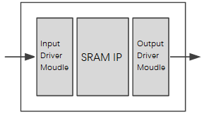
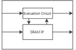
The SRAM hard IP core capacity of the two chips both are 64K (4k x 16bit), the operating voltage is 1.2V, and the maximum operating frequency is 150MHz. The functional block diagrams of the two chips are shown in Figure 4 and Figure 5. The size of these two chips both are 4 997.184μm *3 998.364μm (excluding scribe line). The bonding pad size is 66μm *66μm.


Figure 4.   The functional block diagram of chip A.


Figure 5.   
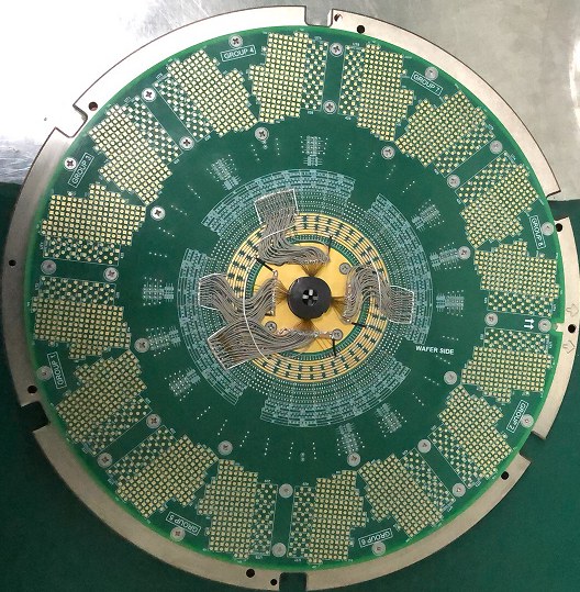
The functional block diagram of chip B.
According to the specific characteristics of the chip and the requirement of timing accuracy, the timing performance of SRAM hard IP core will be tested mainly by using timing edge scanning test, Digitizers sampling analysis, Time-Domain Reflectometry (TDR) timing calibration and compensation and other methods of ATE. The two chips are tested and verified by V93000 tester (made by Advantest Company of Japan). Each PS1600 digital board of the tester has 128 test channels, the depth of test vectors is 112 M lines, the timing resolution is 1 pS, and the timing accuracy is 80 pS. It can effectively support the test of hard IP core timing parameters [15]. The prober card of these two chips is shown in Figure 6.


Figure 6.   
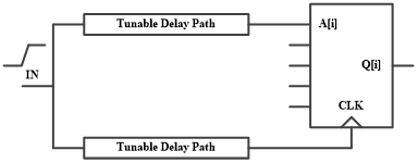
Tested chip prober card.
Chip A and chip B are tested separately. Taking address setup time as an example, chip A adopts the general test method of AC parameters, and the test result is about 1nS. Chip B is tested by ATE combined with evaluation circuit. There are two delay chains DL1 and DL2 in the evaluation circuit, and the delay time can be adjusted by DL1_BSEL_PAD, DL1_LSEL_PAD, DL2_BSEL_PAD and DL2_ LSEL_ PAD these four signals, among which DL1_BSEL_PAD and DL2_LSEL_ PAD signal are used for coarse tuning and DL1_LSEL_PAD and DL2_ LSEL_ PAD signals are used for fine tuning. In the initial state, the delay time of two delay chains is set to be the same, then keep the delay of DL2 unchanged while testing, and increase the delay of DL1 continuously, if the output of SRAM_Q4FSM is 0, the delay between the two delay chains does not satisfy the setup time. When the output becomes 1, the delay satisfies the setup time.
According to the test specifications, power on the chip, set the required pins in high and low states, and float all the rest unused pins, apply address and clock signals to AX_IN_PAD and CLK_IN_PAD. If SRAM_Q4FSM is high level for a period of time, record the values of DL1_BSEL_PAD and DL1_LSEL_PAD respectively, which represents the time of two square wave signals’ timing edge when they can be identified by the edge-triggered D Flip-flop chain in the chip, and then the address setup time of the chip can be calculated. The chip is tested on V93000 test platform. The address setup time test diagram is shown in Figure 7. Through the above test methods, the address setup time parameters of 10 chips (5 chip A and 5 chip B) were tested three times, and the data results are shown in Table 1. The test accuracy of chip A is about nS level while the test accuracy of chip B can reach pS level.


Figure 7.   The address setup time test diagram.
Table 1.   Address setup time test results of the chip.
ChipChip AChip B
No.1234512345
tas (nS)1st1.11.00.91.00.90.85650.78960.70290.81630.7596
2nd1.21.10.90.90.90.83290.71280.72420.80870.7603
3rd1.11.00.91.00.80.84580.76420.70180.82580.7429
Avg.1.131.030.90.970.870.84510.75550.70960.81690.7543
5.   Conclusion
In this paper, a general evaluation system chip simulating user SOC was designed to embed the hard IP core under test. Combined with the external automatic test equipment(ATE)and the on-chip evaluation circuit, a general evaluation system of simulating user system on chip (SOC) with signal timing calibration and compensation by software and hardware compensation structures were introduced to realize the function, performance and reliability verification of the hard IP core. This paper completes the design and verification of SRAM hard IP core verification test based on on-chip evaluation circuit, and realizes the test of AC parameters such as the data setup/hold time, address/control signal setup/hold time of hard IP core. The accuracy of testing the timing parameters of hard IP core can reach pS level, compared with the hard IP core packaged test, the accuracy of the result data is fully reflected.
[1] S W PEI, Z L LI, S L LI et al, “Performance parameter testing for ADC and DAC IP cores without I/O multiplexing in SOC using Verigy 93000”, ACTA Electronica Sinica, 41(7), 1358-1364 (2013).
[2] Y HU, Y H HAN, and X W L I. “Design-for-testability and test technologies for system-on-a-chip”, Journal of Computer Research and Development, 42(1), 153-162 (2005).
[3] ITRS, INTERNATIONAL TECHNOLOGY ROADMAP FOR SEMICONDUCTORS, 2016 Edition, 6-7 (2016).
[4] E N ZHAO, G P SHAO, “Built-in self test technique for testing IP cores”, Microcomputer Information, 21(4), 134-135,17 (2005).
[5] K YU, S Y YE, J H QI, et al., Hard IP Core NDT Architecture and Its Implementation, ZL20141 0597407.7 (2017).
[6] C P XU, J ZHANG, M ZHANG, et al., “Power constraints in SOC test scheduling”, Journal of Guilin University of Electronic Technology, 29(2), 77-81 (2009).
[7] IEEE 1500 Group, 1500-2005-IEEE standard testability method for embedded core based integrated circuits, New York, NY, USA (2005).
[8] E M TAN, P WANG, “Design of the Test Architecture for IP Cores on SoC Based on IEEE 1500 Standard”, Communications in Computer and Information Science, pp.86-94 (2011).
[9] S. H. Goh, Y. H. Chan, L Zhao, et al., “Concurrent built-in self-testing under the constraint of shared test resources and its test time reduction”, Integration, 59(12), 198-205 (2017).
[10] F. R. Rosa, R. M. Brum, G. Wirth et al., “Impact of dynamic voltage scaling and thermal factors on SRAM reliability”. Microelectronics Reliability, 55(12), 1486-1490 (2015).
[11] DEKKER R, BEENKER F, and THIJSSEN L, “Fault modeling and test algorithms for static random access memories”, Proceedings of International Test Conference, Washington, DC, USA, pp.343-352 (1988).
[12] J GAO, “Parallel method of memory test”, Electronic Test, 2009 (2), 47-49 (2009).
[13] C Kuo, W Wei, M Cai, et al., “Efficient defect identification of soft failures induced by device local mismatch for nano-scale SRAM yield improvement”, Materials Science in Semiconductor Processing, 60(3), 79-87 (2017).
[14] Y H LIU, W P JING, “Research and implement of memory diagnostic algorithms”, Electronics & Packaging, 6(12), 23-25,48 (2006).
[15] Advantest Corporation, V93000 Specification (2013).
Article and author information
Kun Yu
Hua Wang
Publication records
Published: June 10, 2019 (Versions2
References
Journal of Microelectronic Manufacturing