Research Article Archive Versions 2 Vol 1 (2) : 18010203 2018
Download
Variational Level-set Formulation for Lithographic Source and Mask Optimization
: 2018 - 11 - 20
: 2018 - 12 - 20
2466 32 0
Abstract & Keywords
Abstract: This paper addresses the contributing factors in lithographic source and mask optimization, namely, the accuracy of the image formation model and the efficiency of the inverse imaging calculations in the optimization framework. A variational level-set formulation is established to incorporate a distance regularization term and an external energy. The former maintains a signed-distance profile and the latter minimizes the sum of the mismatches between the printed image and the desired one over all locations. Hence the need of reinitialization is eliminated in a principle way securing a stable level-set evolution and accurate computation with a simpler and more efficient numerical implementation. We employ a vector imaging model together with a stratified media model to describe the vector nature of electromagnetic fields propagating in the coupling image formation. Several strategies including computing the convolution operation with Fast Fourier Transform, the electric-field caching technique and the conjugate gradient method are discussed to ease the computation load and improve convergence.
Keywords: computational lithography; variational level set; source and mask optimization; coupling image
1.   Introduction
The ever smaller mask feature sizes with increasingly large designs of semiconductor industry call for the development of next-generation lithography simulators and increasingly aggressive optical resolution enhancement techniques (RETs) [1] including modified illumination schemes [2] and optical proximity correction (OPC) [3, 4]. Source mask optimization (SMO) with inverse lithography technology (ILT) [5] generates an ILT-optimized mask for each designated illumination with the best combination of source and mask to compensate for the optical diffraction error introduced by the band-limited imaging system, enabling the continuation of the current immersion lithography.
The goal of the SMO is to transfer designed circuit patterns onto silicon wafers, whose performance is heavily dependent on the accuracy of image formation model and the efficiency of the inverse imaging calculation. Over the years, the evolvement of the lithography systems has witnessed the extension from scalar imaging models which are only accurate for systems with low numerical apertures (NAs) less than \(0.4\) [6] to vector imaging models. The development of vector imaging can be tracked back from the long celebrated classics by Born and Wolf [7], through the revised format of the Hopkins formulation by Yeung [6], Flagello [8], Pistor [9] and the resist vector model by Adam et al. [10] to the consistent high-NA optics by Peng [11]. Together with the development of illuminations source representations from the arc decomposition [12], the meshpoint representation [13] to pixelated sources by customized diffractive optical element (DOE) [14], various SMO approaches based on scalar imaging model including gradient methods [15-17], augmented Lagrangian [18] and alike, are given impetus to include vector imaging formation tracking the polarization state as light propagates through the optical components of the projection instruments [17]. Meanwhile, level-set approaches have been actively explored in [19, 20] solving inverse lithography problems, and systematic level-set implementations with appropriate finite-difference schemes are presented in scalar [21-23] and vector imaging systems [24, 25] for photomask synthesis problems. However, the coupling images in these frameworks are usually assumed to be aerial images, while in optical projection lithography intensity distribution within the photoresist or the resist images should be used to account for the transmission and reflection through the dielectric film stack.
In this paper, we present a variational level-set formulation for the source and mask optimization incorporating a regularization energy term preserving the signed distance property combined with an external energy seeking the minimization of the properly designed cost functions to improve pattern fidelity, securing stable level-surface evolution and computation accuracy and eliminating the need of reinitialization. The underlying vector imaging formation is combined with a stratified media model to account for the vector nature of electromagnetic field propagation in the lithography system and to track the reflection from and transmission through the wafer stack. The level-set formulation is reduced to a time-dependent model which is subsequently solved with Polak-Ribiệre-Polyak (PRP) conjugate gradient (CG) method to improve convergence performance. Electrical field caching technique (EFCT) and fast fourier transform (FFT) are employed to significantly reduce the computation load.
2.   Variational Level-set Formulation for SMO
With \(\mathrm{N}\) and \({\mathrm{N}}_{\mathrm{s}}\mathrm{ }\)being the sizes of the discretized mask and source matrices, given a target pattern \({\mathbf{I}}_{0}\in {\mathcal{R}}^{\mathrm{N}×\mathrm{N}}\), the goal of the SMO is to find the optimal source \(\hat{\mathbf{J}}\in {{R}^{{{N}_{S}}\times {{N}_{S}}}}\) and mask pattern \(\hat{\mathbf{M}}\in {{R}^{N\times N}}\), which minimizes a designed distance between \(\mathcal{T}\left\{\bullet \right\}\) and \({\mathbf{I}}_{0}\), namely
\(\left( \hat{\mathbf{J}},\hat{\mathbf{M}} \right)=\underset{\hat{J}\in {{R}^{{{N}_{S}}\times {{N}_{S}}}},\hat{M}\in {{R}^{N\times N}}}{\mathop{\min }}\,d\left\{ {{I}_{0}},\mathcal{T}\left\{ \mathbf{J},\mathbf{M} \right\} \right\}\) , (1)
with \(\mathrm{d}\left\{\bullet ,\bullet \right\}\) being an appropriately defined distance metric and \(\mathcal{T}\left\{\bullet \right\}\) being the forward imaging formation.
2.1.   Level-set Optimization Framework
We give \(\mathbf{J}\) and \(\mathbf{M}\) a level-set description by introducing unknown functions \({\mathrm{\varphi }}_{\mathbf{J}}\) and \({\mathrm{\varphi }}_{\mathbf{M}}\), respectively which relate to \(\mathbf{J}\) and \(\mathbf{M}\) as
\(\mathbf{J}=\left\{ \begin{matrix} {{j}_{\operatorname{int}}}for\left\{ r:{{\Phi }_{J}}\left( r \right)<0 \right\} \\ {{j}_{out}}for\left\{ r:{{\Phi }_{J}}\left( r \right)>0 \right\} \\\end{matrix} \right.,and\ \ \mathbf{M}=\left\{ \begin{matrix} {{m}_{\operatorname{int}}}for\left\{ r:{{\Phi }_{M}}\left( r \right)<0 \right\} \\ {{m}_{out}}for\left\{ r:{{\Phi }_{M}}\left( r \right)>0 \right\} \\\end{matrix} \right.\) (2)
where \(\mathbf{r}\) denotes spatial coordinate \(\left(\mathrm{x},\mathrm{y}\right)\), \({\mathrm{j}}_{\mathrm{i}\mathrm{n}\mathrm{t}}\), \({\mathrm{m}}_{\mathrm{i}\mathrm{n}\mathrm{t}}\) are predefined negative numbers and \({\mathrm{j}}_{\mathrm{o}\mathrm{u}\mathrm{t}}\), \({\mathrm{m}}_{\mathrm{o}\mathrm{u}\mathrm{t}}\) are predefined positive numbers for binary source and mask patterns. Consequently, the inverse lithography problem of SMO is reformulated to handle the level set functions (LSFs) \({{\Phi }}_{\mathbf{J}}\) and \({{\Phi }}_{\mathbf{M}}\) instead of the source and mask patterns \(\mathbf{J}\) and \(\mathbf{M}\).
With the synthesized source and mask patterns \(\hat{J}\) and \(\hat{M}\) embedded as the evolution of zero level set of \({{\Phi }}_{\mathbf{J}}\) and \({{\Phi }}_{\mathbf{M}}\), it is necessary to maintain \({\Phi }_{\mathbf{J}}\) and \({\Phi }_{\mathbf{M}}\) in good conditions, so that the level set evolution is stable and the numerical computation is accurate, which is well satisfied by the signed distance property \(\left|\nabla {{\Phi }}_{\mathbf{i}}\right|=1,\mathrm{ }\mathbf{i}=\mathbf{J}\mathrm{ }\ \mathrm{o}\mathrm{r}\ \mathrm{ }\mathbf{M}\)[26] , where \(\nabla \) is the gradient operation. In conventional level set formulations, the LSFs \({\Phi }_{\mathbf{J}}\) and \({\Phi }_{\mathbf{M}}\) are typically initialized and periodically reinitialized as a signed distance function by solving the evolution equation to steady state [27]
\(\frac{\partial \mathrm{\psi }}{\partial \mathrm{t}}=\mathrm{s}\mathrm{i}\mathrm{g}\mathrm{n}\left({\mathrm{\varphi }}_{\mathbf{i}}\right)\left(1-\left|\nabla \mathrm{\psi }\right|\right),\mathrm{ }\mathbf{i}=\mathbf{J}\mathrm{ }\mathrm{o}\mathrm{r}\mathrm{ }\mathbf{M},\) (3)
yet fundamental problem as when and how to practice reinitialization remains [28].
2.1.1.   Level-set Optimization Framework
To keep the evolving \(\mathbf{J}\) and \(\mathbf{M}\) as signed distance functions especially in the vicinity of the zero level set, we define an energy function \(\mathcal{E}\left({\Phi }\right)\) of the LSF \({\Phi }\) by
\(\mathcal{E}\left({\Phi }\right)=\mathrm{\mu }{\mathcal{R}}_{\mathcal{P}}\left({\Phi }\right)+{\mathcal{E}}_{\mathrm{e}\mathrm{x}\mathrm{t}}\left({\Phi }\right)\) , (4)
where \({\mathcal{R}}_{\mathcal{P}}\left({\Phi }\right)\) is the distance regularized level set (DRLS) term [26, 29], \(\mathrm{\mu }\) is a constant and \({\mathcal{E}}_{\mathrm{e}\mathrm{x}\mathrm{t}}\left({\Phi }\right)\) is the external energy term that minimizes the the designed distance \(\mathrm{d}\left\{\bullet ,\bullet \right\}\) in Equation (1). It should be noticed that we will drop the subscript \(\mathbf{i}=\mathbf{J}\mathrm{ }\ \mathrm{o}\mathrm{r}\ \mathrm{ }\mathbf{M}\) of the LSF \({\Phi }\) without ambiguity to denote the same actions of \({\Phi }_{\mathbf{J}}\) and \({\Phi }_{\mathbf{M}}\), unless specified otherwise. The DRLS term is formulated as
\({\mathcal{R}}_{\mathcal{P}}\left({\Phi }\right)\triangleq {\int }_{\mathrm{\Omega }\in {\mathcal{R}}^{\mathrm{N}×\mathrm{N}}}^{}\mathcal{P}\left(\left|\nabla {\Phi }\right|\right)d\mathbf{r}\) , (5)
where \(\mathcal{P}\left(\bullet \right):\left[0,\mathrm{ }\mathrm{\infty }\right]\to \mathcal{R}\) is a potential function [26, 29], which is defined naturally as
\(\mathcal{P}\left({\Phi }\right)={\int }_{\mathrm{\Omega }}^{}\frac{1}{2}{\left(\left|\nabla {\Phi }\right|-1\right)}^{2}d\mathbf{r}.\) (6)
The level-set formulation in Equation (4) has an intrinsic capability of maintaining regularity of the level set function, ensuring a stable evolution of \({\Phi }\) without the necessity of reinitialization, which is an iterative process and could be time consuming.
The standard method to minimize an energy function \(\mathcal{E}\left({\Phi }\right)\) in Equation (4) is to find the steady state solution of the gradient flow equation
\(\frac{\partial {\Phi }}{\partial \mathrm{t}}=-\frac{\partial \mathcal{E}}{\partial {\Phi }},\) (7)
where \(\frac{\partial \mathcal{E}}{\partial {\Phi }}\) is the Gâteaux derivative of the functional \(\mathcal{E}\). Equation (7) is an evolution equation of a time-dependent function \({\Phi }\left(\mathbf{r},\mathrm{ }\mathrm{t}\right)\) with a spatial variable \(\mathbf{r}\) in the domain\(\mathrm{\Omega }\in {\mathcal{R}}^{\mathrm{N}×\mathrm{N}}\) and a temporal variable\(\mathrm{ }\mathrm{t}\). The evolution starts with a given initial function \({\Phi }\left(\mathbf{r},\mathrm{ }0\right)={{\Phi }}_{0}\left(\mathbf{r}\right)\). Consequently, the wafer imaging formation \(\mathcal{T}\left\{\bullet \right\}\) should be formatted to compute the Gâteaux derivative of \({\mathcal{E}}_{\mathrm{e}\mathrm{x}\mathrm{t}}\left({\Phi }\right)\) with respect to \({\Phi }\).
2.2.   Wafer Image Formation
The lithographic process \(\mathcal{T}\left\{\bullet \right\}\) in Equation (1) is divided into two function blocks, namely, the projection optics effects (coupling image formation) and resist effects, a schematic of which is given in Figure 1. In optical projection lithography, the apposite image is formed in the photoresist, which is an organic, light-absorbing layer within a stack of materials coated on a silicon wafer. Energy is


Figure 1.   Projection optics in a vector imaging model.
deposited into the photoresist by electromagnetic wave coupling through the wafer stack to form the resist image. Similar to the case of the mask near-field, rigorous Maxwell-equation solvers are also required to account for the amplitudes and propagation angle changes of the light rays in the wafer stack. Although topography on a wafer is in general irregular, with most layers in modern integrated circuits being planarized, it is appropriate to approximate the wafer stack as stratified media in which the material properties vary only in the \(\mathrm{z}\)-direction, as depicted in Figure 2.


Figure 2.   Reflection from and transmission through a stratified medium.
For a point source \(\left({\mathrm{\alpha }}_{\mathrm{s}},{\mathrm{\beta }}_{\mathrm{s}}\right)\) emanating a monochromactic wave, the coupling image formation is defined by the Fraunhofer diffraction [31], the conservation of energy for ideal lenses between the entrance and the exit pupil and the Abbe's source integration approach [7] for partially illumination systems to give
\({\mathbf{I}}_{\mathrm{p}\mathrm{r}}=\frac{1}{{\mathrm{N}}_{\mathrm{s}}}\sum _{{\mathrm{\alpha }}_{\mathrm{s}}}\sum _{{\mathrm{\beta }}_{\mathrm{s}}}\sum _{\mathrm{p}=\mathrm{x},\mathrm{y},\mathrm{z}}{‖{\mathbf{H}}_{\mathrm{p}}\left({\mathrm{\alpha }}_{\mathrm{s}},{\mathrm{\beta }}_{\mathrm{s}}\right)\otimes \mathbf{B}\left({\mathrm{\alpha }}_{\mathrm{s}},{\mathrm{\beta }}_{\mathrm{s}}\right)⨀\mathbf{M}‖}^{2},\mathrm{ }\) (8)
where \({\mathrm{N}}_{\mathrm{s}}\) is the number of source points, \({\mathbf{H}}_{\mathrm{p}}\), \(\mathbf{B}\) are functions of \(\left({\mathrm{\alpha }}_{\mathrm{s}},{\mathrm{\beta }}_{\mathrm{s}}\right)\), \(\otimes \) denotes convolution operation and \(⨀\) is the entry-by-entry multiplication. \({\mathbf{H}}_{\mathrm{p}}\left({\mathrm{\alpha }}_{\mathrm{s}},{\mathrm{\beta }}_{\mathrm{s}}\right),\mathrm{ }\mathrm{p}=\mathrm{x},\mathrm{ }\mathrm{y},\mathrm{ }\mathrm{z}\) are referred to as the equivalent filters of the \(\mathrm{x},\mathrm{ }\mathrm{y},\mathrm{ }\mathrm{z}\) components and \(\mathbf{B}\in {\mathcal{R}}^{\mathrm{N}×\mathrm{N}}\) is the diffraction matrix under the constant scattering coefficient assumption (CSCA) [30].
The resist effect can be approximated using a logarithmic sigmoid function \(sig\left(\mathrm{x}\right)=\frac{1}{1+{\mathrm{e}}^{-\mathrm{a}\left(\mathrm{x}-{\mathrm{t}}_{\mathrm{r}}\right)}}\) with \(\mathrm{a}\) being the steepness of the sigmoid function and \({\mathrm{t}}_{\mathrm{r}}\) being the threshold. Putting together, we can write the wafer imaging formation \(\mathcal{T}\left\{\bullet \right\}\) as
\(\mathbf{I}=\mathcal{T}\left\{\mathbf{M}\right\}=sig\left({\mathbf{I}}_{\mathrm{p}\mathrm{r}}\right)= sig\left(\frac{1}{{\mathrm{N}}_{\mathrm{s}}}\sum _{{\mathrm{\alpha }}_{\mathrm{s}}}\sum _{{\mathrm{\beta }}_{\mathrm{s}}}\sum _{\mathrm{p}=\mathrm{x},\mathrm{y},\mathrm{z}}{‖{\mathbf{H}}_{\mathrm{p}}\left({\mathrm{\alpha }}_{\mathrm{s}},{\mathrm{\beta }}_{\mathrm{s}}\right)\otimes \mathbf{B}\left({\mathrm{\alpha }}_{\mathrm{s}},{\mathrm{\beta }}_{\mathrm{s}}\right)⨀\mathbf{M}‖}^{2}\right).\) (9)
Due to diffraction, \(\mathbf{I}\) is necessarily a distorted version of a given target pattern, which has to be compensated by computational lithography techniques to achieve a desired printed pattern. With the forward imaging \(\mathcal{T}\left\{\bullet \right\}\) defined, the level-set time-dependent model can be derived.
2.3.   The Time-dependent Model
The gradient flow of the \(\mathcal{E}\left({\Phi }\right)\) is
\(\frac{\partial {\Phi }}{\partial \mathrm{t}}=-\mathrm{\mu }\frac{\partial {\mathcal{R}}_{\mathcal{P}}}{\partial {\Phi }}-\frac{\partial {\mathcal{E}}_{\mathrm{e}\mathrm{x}\mathrm{t}}}{\partial {\Phi }},\mathrm{ }\) (10)
where the Gâteaux derivative of \({\mathcal{R}}_{\mathcal{P}}\) in Equation (13) is given as [26]
\(\frac{\partial {\mathcal{R}}_{\mathcal{P}}}{\partial {\Phi }}=-\nabla \bullet \left({d}_{\mathcal{P}}\left(\left|\nabla {\Phi }\right|\right)\nabla {\Phi }\right),\mathrm{ }\mathrm{ }\mathrm{ }\mathrm{ }\) (11)
and \({d}_{\mathcal{P}}\) defined as
\({d}_{\mathcal{P}}\left(\left|\nabla {\Phi }\right|\right)=\frac{{\mathcal{P}}^{\mathrm{\text{'}}}\left(\left|\nabla {\Phi }\right|\right)}{\left|\nabla {\Phi }\right|}\) . (12)
Combining with Equation (6), the variational formulation in Equation (13) can be further expressed as
\(\frac{\partial{\Phi }}{\partial \mathrm{t}}=\mathrm{\mu }\left[∆{\Phi }-\nabla \bullet \left(\frac{\nabla{\Phi }}{\left|\nabla{\Phi }\right|}\right)\right]-\frac{\partial {\mathcal{E}}_{\mathrm{e}\mathrm{x}\mathrm{t}}}{\partial {\Phi }},\) (13)
with \(∆\) being the Laplacian operation.
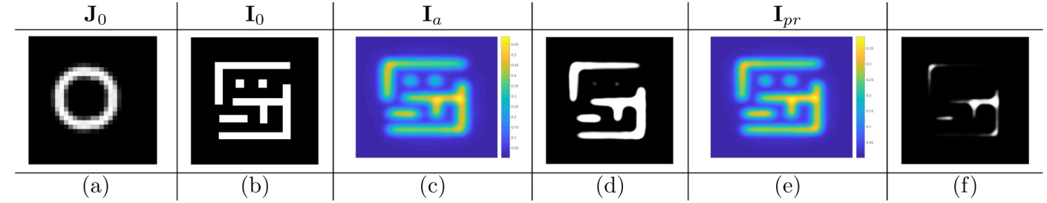
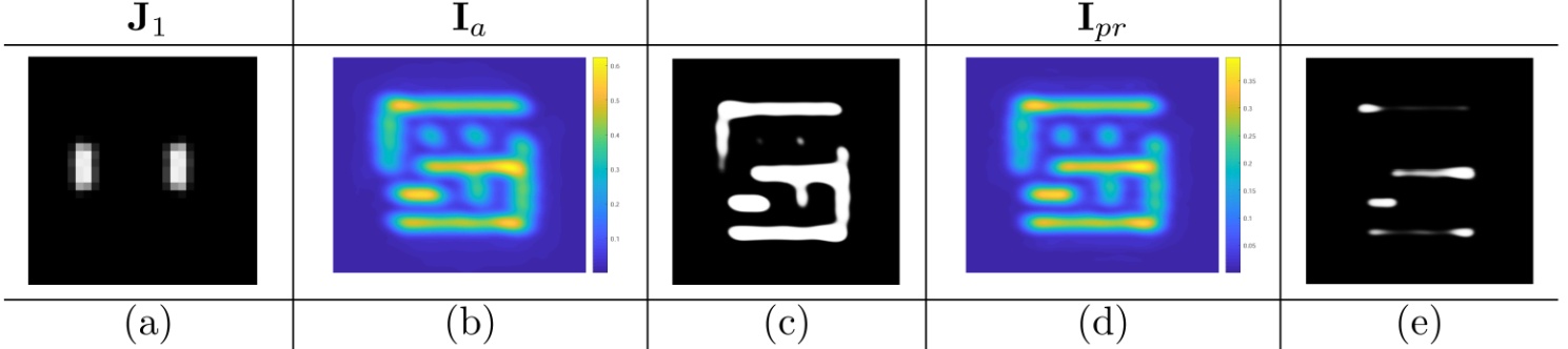
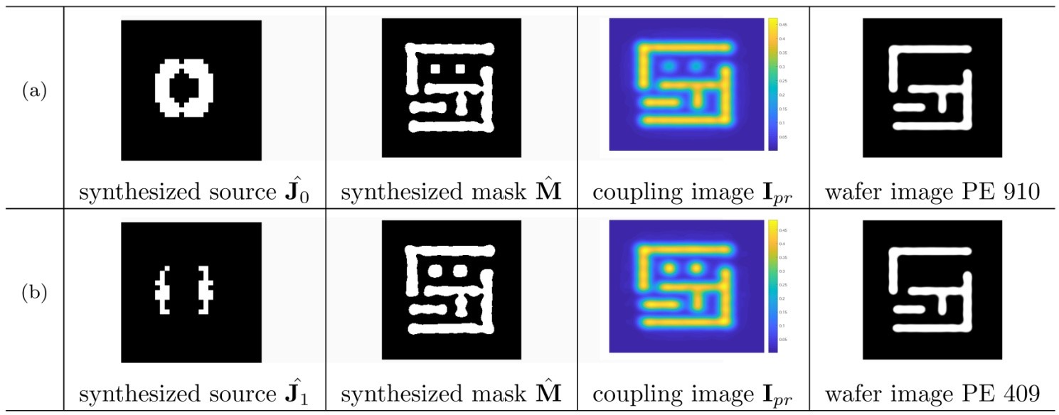
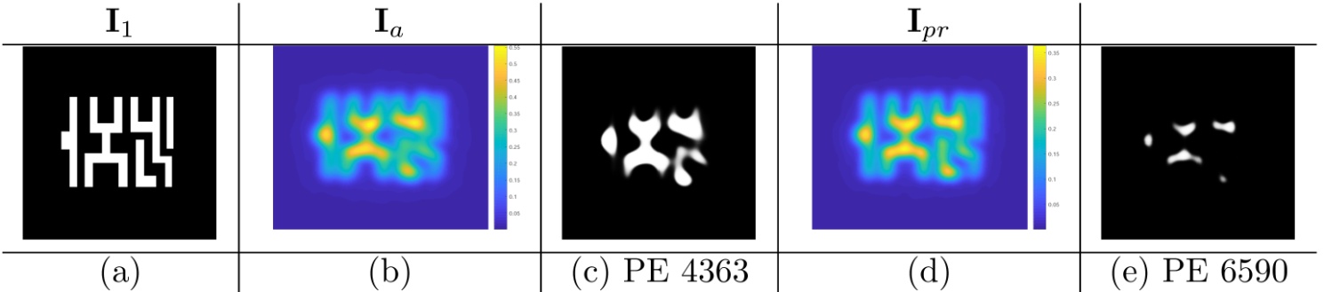
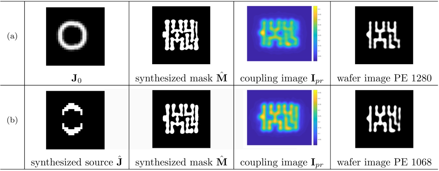
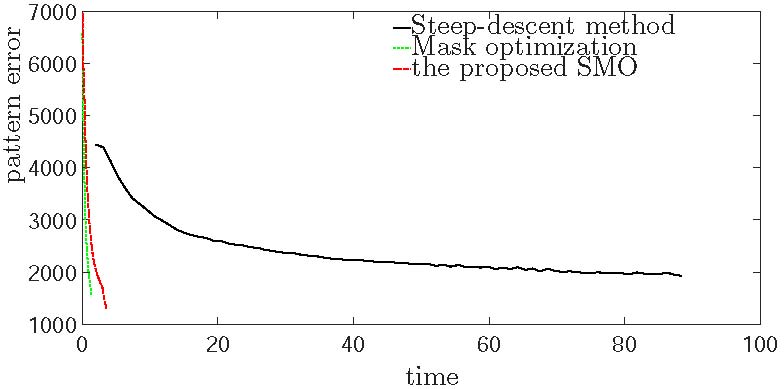
From Reference [25], it is noted that the edge placement error (EPE) has a positive relationship with the pattern error which is the sum of the mismatches between the printed image and the desired one over all locations in general. However, explicit incorporation of the EPE into the cost functions is often too complicated. Therefore, in this paper the distance metric \(\mathrm{d}\left\{\bullet ,\bullet \right\}\) in Equation (1) is defined as the pattern error (PE) to show the validity of the proposed variational level-set based SMO method. However, other distance metrics including EPE, process variation (PV) band and their combinations could be incorporated into the cost functions. Minimizing the external energy term \({\mathcal{E}}_{\mathrm{e}\mathrm{x}\mathrm{t}}\) relates to solving Equation (1) with a least squares seeking the minimizer of
\(\mathrm{F}\left(\mathbf{J},\mathrm{ }\mathbf{M}\right)=\frac{1}{2}{‖\mathcal{T}\left\{\mathbf{J},\mathrm{ }\mathbf{M}\right\}-{\mathbf{I}}_{0}‖}^{2},\mathrm{ }\mathrm{ }\mathrm{ }\mathrm{ }\) (14)
where \(‖\bullet ‖\) stands for the \({\mathcal{l}}_{2}\) norm. The source and mask co-optimization approach updates both \(\mathbf{J}\) and \(\mathbf{M}\) in each iteration, which is explicitly revealed by the evolution of level surfaces represented by the time-dependent models with respect to and \({\Phi }\), namely,
\(\frac{\partial {{\Phi }}_{\mathbf{i}}}{\partial \mathrm{t}}=-\left|\nabla {{\Phi }}_{\mathbf{i}}\right|{\mathcal{v}}_{\mathbf{i}}\left(\mathbf{r},\mathrm{ }\mathrm{t}\right),\mathrm{ }\mathbf{i}=\mathbf{J}\mathrm{ }\ \mathrm{o}\mathrm{r}\ \mathrm{ }\mathbf{M},\) (15)
In which \({\mathcal{v}}_{\mathrm{J}}\left(\mathbf{r},\mathrm{ }\mathrm{t}\right)\) and \({\mathcal{v}}_{\mathbf{M}}\left(\mathbf{r},\mathrm{ }\mathrm{t}\right)\) are the velocity functions normal to the surfaces of \({\Phi }_{\mathbf{J}}\) and \({\Phi }_{\mathbf{M}}\), respectively, and are defined as
\({\mathcal{v}}_{\mathrm{J}}\left(\mathbf{r},\mathrm{ }\mathrm{t}\right)=-{\mathcal{J}\left\{\mathbf{J}\right\}}^{\mathrm{T}}\left(\mathcal{T}\left\{\mathbf{J}\right\}-{\mathbf{I}}_{0}\right)=\frac{1}{2}\frac{\mathrm{\vartheta }}{\mathrm{\vartheta }\mathbf{J}}{\left(\mathbf{I}-{\mathbf{I}}_{0}\right)}^{2}=2\mathrm{a}\sum _{{\mathrm{\alpha }}_{\mathrm{s}},{\mathrm{\beta }}_{\mathrm{s}}}\frac{\sum _{\mathrm{p}=\mathrm{x},\mathrm{y},\mathrm{z}}{‖{\mathbf{E}}_{\mathrm{p}}\left({\mathrm{\alpha }}_{\mathrm{s}},{\mathrm{\beta }}_{\mathrm{s}}\right)‖}^{2}-{\mathbf{I}}_{\mathrm{a}}}{\sum _{{\mathrm{\alpha }}_{\mathrm{s}},{\mathrm{\beta }}_{\mathrm{s}}}\mathbf{J}}⨀\left({\mathbf{I}}_{0}-\mathbf{I}\right)⨀\mathbf{I}⨀\left(1-\mathbf{I}\right)\) , (16)
and
\({\mathcal{v}}_{\mathrm{M}}\left(\mathbf{r},\mathrm{ }\mathrm{t}\right)=-{\mathcal{J}\left\{\mathbf{M}\right\}}^{\mathrm{T}}\left(\mathcal{T}\left\{\mathbf{M}\right\}-{\mathbf{I}}_{0}\right)=\frac{1}{2}\frac{\mathrm{\vartheta }}{\mathrm{\vartheta }\mathbf{M}}{\left(\mathbf{I}-{\mathbf{I}}_{0}\right)}^{2}=-\frac{2\mathrm{a}}{\sum _{{\mathrm{\alpha }}_{\mathrm{s}},{\mathrm{\beta }}_{\mathrm{s}}}\mathbf{J}}\sum _{{\mathrm{\alpha }}_{\mathrm{s}},{\mathrm{\beta }}_{\mathrm{s}}}\sum _{\mathrm{p}=\mathrm{x},\mathrm{y},\mathrm{z}}\mathbf{J}\left({\mathrm{\alpha }}_{\mathrm{s}},{\mathrm{\beta }}_{\mathrm{s}}\right)\)\(\mathrm{R}\mathrm{e}\mathrm{a}\mathrm{l}\left[{\left(\mathbf{B}\right)}^{\mathrm{*}}⨀\left({\left({\mathbf{H}}_{\mathrm{p}}^{\mathrm{*}}\right)}^{\diamond }\left\{{\mathbf{E}}_{\mathrm{p}}\left({\mathrm{\alpha }}_{\mathrm{s}},{\mathrm{\beta }}_{\mathrm{s}}\right)⨀\left({\mathbf{I}}_{0}-\mathbf{I}\right)⨀\mathbf{I}⨀\left(1-\mathbf{I}\right)\right\}\right)\right]\mathrm{ }\) , (17)
with \(\mathcal{J}\left\{\bullet \right\}\) being the Jacobian, \(\mathrm{*}\) being the conjugate operation, \(\diamond \) flipping the matrix in the argument in both up-down and right-left directions, \(1\in {\mathcal{R}}^{\mathrm{N}×\mathrm{N}}\) being the all-ones matrix and \({\mathbf{E}}_{\mathrm{p}}\left({\mathrm{\alpha }}_{\mathrm{s}},{\mathrm{\beta }}_{\mathrm{s}}\right)={\mathbf{H}}_{\mathrm{p}}\left({\mathrm{\alpha }}_{\mathrm{s}},{\mathrm{\beta }}_{\mathrm{s}}\right)\otimes \mathbf{B}\left({\mathrm{\alpha }}_{\mathrm{s}},{\mathrm{\beta }}_{\mathrm{s}}\right)⨀\mathbf{M}\). Putting back into Equation (16) yields
\(\frac{\partial {{\Phi }}_{\mathbf{i}}}{\partial \mathrm{t}}=\mathrm{\mu }\left|\nabla {{\Phi }}_{\mathbf{i}}\right|\left[∆{{\Phi }}_{\mathbf{i}}-\nabla \bullet \left(\frac{\nabla {{\Phi }}_{\mathbf{i}}}{\left|\nabla {{\Phi }}_{\mathbf{i}}\right|}\right)\right]-\left|\nabla {{\Phi }}_{\mathbf{i}}\right|{\mathcal{v}}_{\mathbf{i}}\left(\mathbf{r},\mathrm{ }\mathrm{t}\right)={-\left|\nabla {{\Phi }}_{\mathbf{i}}\right|\mathrm{g}}_{\mathbf{i}}\left(\mathbf{r},\mathrm{ }\mathrm{t}\right),\mathrm{ }\mathbf{i}=\mathbf{J}\ \mathrm{ }\mathrm{o}\mathrm{r}\ \mathrm{ }\mathbf{M},\) (18)
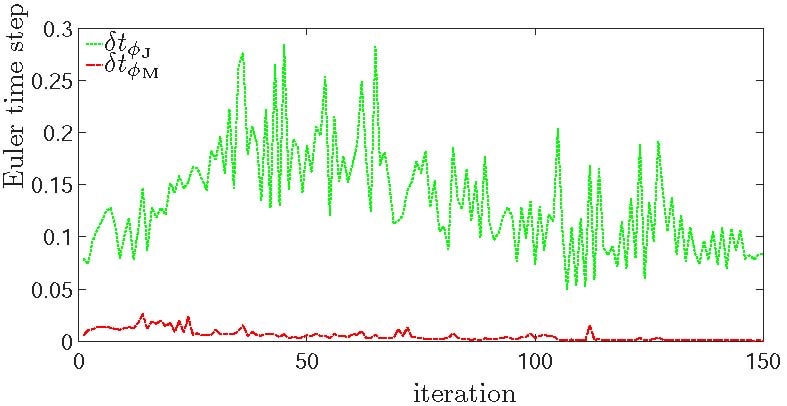
where \({\mathrm{g}}_{\mathbf{i}}\left(\mathbf{r},\mathrm{ }\mathrm{t}\right)=\mathrm{\mu }\left(∆{{\Phi }}_{\mathbf{i}}-{\mathcal{v}}_{\mathbf{i}}-\nabla \bullet \left(\frac{\nabla {{\Phi }}_{\mathbf{i}}}{\left|\nabla {{\Phi }}_{\mathbf{i}}\right|}\right)\right)\). In Equation (18), the gradient magnitude \(\left|\nabla {\Phi }\right|\) is multiplied to the right hand side of the equation, which accelerates the movement of the level curves of \({\Phi }\) and regularizes the parabolic term in a nonlinear way [21]. Generally, for convergence and stability, Courant-Friedrichs-Lewy (CFL) condition [33] is often applied asserting that the numerical wave speed must be at least as fast as the physical wave, giving
\(\mathrm{\delta }\mathrm{t}\bullet \mathrm{m}\mathrm{a}\mathrm{x}\left\{\frac{\left|{\mathrm{g}}_{\mathrm{x}}\right|}{\mathrm{\delta }\mathrm{x}}+\frac{\left|{\mathrm{g}}_{\mathrm{y}}\right|}{\mathrm{\delta }\mathrm{y}}\right\}=\mathrm{\epsilon },\) (19)
where \(\mathrm{\delta }\mathrm{x}\) and \(\mathrm{\delta }\mathrm{y}\) are the grid size of the discrete Cartesian grid, \({\mathrm{g}}_{\mathrm{x}}\) and \({\mathrm{g}}_{\mathrm{y}}\) are the components of \(\mathrm{g}\) in the \(\mathrm{x}\) and \(\mathrm{y}\) direction, \(0<\mathrm{\epsilon }<1\mathrm{ }\)is the CFL number and\(\mathrm{\delta }\mathrm{t}\) is the Euler time step, which for numerically stability is evaluated in every iteration.
3.   Efficiency Enhancing Strategies
It is observed that in Equations (9), (16) and (17), the complexity of the convolution operation is superlinear with respect to \(\mathrm{N}\), which is much more computational expensive than the entry-by-entry multiplication. Therefore the major computation load in updating the mask pattern is invoked by the convolution operations. The first strategy to ease the computation load is referred to as the electric-field caching technique (EFCT) [17, 25], where \({\mathbf{E}}_{\mathrm{p}}\left({\mathrm{\alpha }}_{\mathrm{s}},{\mathrm{\beta }}_{\mathrm{s}}\right)\) is computed only once in each iteration for the computation of the aerial image \({\mathbf{I}}_{\mathrm{a}}\) and is cached in the memory for the later computation of \({\mathcal{v}}_{\mathbf{i}}\left(\mathbf{r},\mathrm{ }\mathrm{t}\right)\), hence a tradeoff of extra memory to save \({\mathrm{N}}_{\mathrm{s}}×\mathrm{N}×\mathrm{N}\) matrices is made for fast computation. The computation intensity can be further reduced by applying the Fast Fourier Transfrom (FFT) to remove the convolution operations by implementing them in the frequency domain where \({\mathbf{E}}_{\mathrm{p}}\) is computed as \({\mathcal{F}}^{-1}\left[\mathcal{F}\left({\mathbf{H}}_{\mathrm{p}}\right)\mathcal{F}\left(\mathbf{B}⨀\mathbf{M}\right)\right]\) in Equations (9) and (16), while Equation (17) is rewritten as
\({\mathcal{v}}_{\mathbf{M}}\left(\mathrm{r},\mathrm{t}\right)=-\frac{2\mathrm{a}}{{\mathrm{N}}_{\mathrm{s}}}\sum _{{\mathrm{\alpha }}_{\mathrm{s}},{\mathrm{\beta }}_{\mathrm{s}}}\sum _{\mathrm{p}=\mathrm{x},\mathrm{y},\mathrm{z}}\mathrm{R}\mathrm{e}\mathrm{a}\mathrm{l}\left[{\left(\mathbf{B}\right)}^{\mathrm{*}}⨀{\mathcal{F}}^{-1}\left\{\mathcal{F}\left[{\left({\mathbf{H}}_{\mathrm{p}}^{\mathrm{*}}\right)}^{\diamond }\right]⨀\mathcal{F}\left[{\mathbf{E}}_{\mathrm{p}}⨀\left({\mathbf{I}}_{0}-\mathbf{I}\right)⨀\mathbf{I}⨀\left(1-\mathbf{I}\right)\right]\right\}\right].\)
In this paper, we update mask by employing the widely used Polak-Ribiệre-Polyak (PRP) conjugate gradient (CG) [34] which is believed most efficient, instead of the steepest descent (SD) practiced in Reference [21, 23, 24] to achieve faster convergence and improved performance, where the evolution velocity \(\mathrm{G}\left(\mathbf{r},\mathrm{ }{\mathrm{t}}_{\mathrm{k}}\right)\) in the \(\mathrm{k}\)th iteration is calculated according to Equation (18) as
\(G\left( r,{{t}_{k}} \right)=\left\{ \begin{matrix} g\left( r,{{t}_{k}} \right)+\eta _{k}^{PRP}\cdot G\left( r,{{t}_{k-1}} \right) \\ g\left( r,{{t}_{k}} \right) \\\end{matrix} \right.\begin{matrix} if\ \ k\ge 1 \\ if\ \ k=0 \\\end{matrix},\) (20)
with \({\mathrm{\eta }}_{\mathrm{k}}^{\mathrm{P}\mathrm{R}\mathrm{P}}\) calculated as
\({\mathrm{\eta }}_{\mathrm{k}}^{\mathrm{P}\mathrm{R}\mathrm{P}}=\frac{{\mathrm{g}\left(\mathbf{r},\mathrm{ }{\mathrm{t}}_{\mathrm{k}}\right)}^{2}-\sum \mathrm{g}\left(\mathbf{r},\mathrm{ }{\mathrm{t}}_{\mathrm{k}}\right)\bullet \mathrm{g}\left(\mathbf{r},\mathrm{ }{\mathrm{t}}_{\mathrm{k}-1}\right)}{{\mathrm{g}\left(\mathbf{r},\mathrm{ }{\mathrm{t}}_{\mathrm{k}-1}\right)}^{2}},\) (21)
The update of the time-dependent \({\Phi }\left(\mathbf{r},\mathrm{t}\right)\) can be implemented by available first-order temporal accurate and second-order accurate spatial finite-difference schemes [21]. With \({\Phi }\left(\mathbf{r},\mathrm{t}\right)\) discretized as \({{\Phi }}_{\mathrm{i},\mathrm{j}}^{\mathrm{k}}\) using spatial index \(\left(\mathrm{i},\mathrm{j}\right)=1,\mathrm{ }\cdots ,\mathrm{ }\mathrm{N}\) and temporal index \(\mathrm{k}\), the level-set equation in Equation (13) can be expressed as
\({{\Phi }}_{\mathrm{i},\mathrm{j}}^{\mathrm{k}+1}={{\Phi }}_{\mathrm{i},\mathrm{j}}^{\mathrm{k}}+\mathrm{\delta }\mathrm{t}\bullet L\left({{\Phi }}_{\mathrm{i},\mathrm{j}}^{\mathrm{k}}\right), k=0, 1, 2, \cdots , \) (22)
which is a iteration process with \(L\left({{\Phi }}_{\mathrm{i},\mathrm{j}}^{\mathrm{k}}\right)\) being a discretized approximation of \({-\left|\nabla {{\Phi }}_{\mathbf{i}}\right|\mathrm{g}}_{\mathbf{i}}\left(\mathbf{r},\mathrm{ }\mathrm{t}\right)\) in Equation (18) and\(\mathrm{ }\mathrm{\delta }\mathrm{t}\) being the time step. The updating procedure of level-set based PRP-CG method for the proposed SMO approach is described in Table 1
Table 1.   The main workflow of the proposed SMO approach
Step1Initialize \({\Phi }_{\mathbf{M}}\) as the desired pattern \({\mathbf{I}}_{0}\) and \({\Phi }_{\mathbf{J}}\) as the initial source pattern \({\mathbf{J}}_{0}\); set the maximum iteration number \(\mathcal{N}\) and the current iteration number \(\mathrm{k}=0\); calculate \({\mathrm{G}}_{\mathbf{i}}\left(\mathbf{r},\mathrm{ }0\right)={\mathrm{g}}_{\mathbf{i}}\left(\mathbf{r},\mathrm{ }0\right)\) in Equation (21) for \(\mathbf{i}=\mathbf{J}\mathrm{ }\mathrm{o}\mathrm{r}\mathrm{ }\mathbf{M}\).
Step2Calculate Euler time step \({\mathrm{\delta }\mathrm{t}}_{{{\Phi }}_{\mathbf{M}}}\) and \({\mathrm{\delta }\mathrm{t}}_{{{\Phi }}_{\mathbf{J}}}\) in Equation (19).
Step3Update \({\Phi }_{\mathbf{M}}\) and \({\Phi }_{\mathbf{J}}\), \({{\Phi }}_{\mathrm{i},\mathrm{j}}^{\mathrm{k}+1}={{\Phi }}_{\mathrm{i},\mathrm{j}}^{\mathrm{k}}+\mathrm{\delta }\mathrm{t}\bullet L\left({{\Phi }}_{\mathrm{i},\mathrm{j}}^{\mathrm{k}}\right)\) in Equation (22).
Step4Update \(M\left( r,k-1 \right)=\left\{ \begin{matrix} {{m}_{\operatorname{int}}}for\left\{ r:{{\Phi }_{M}}\left( r \right)<0 \right\} \\ {{m}_{out}}for\left\{ r:{{\Phi }_{M}}\left( r \right)>0 \right\} \\ \end{matrix} \right.\) and\(J\left( k,k-1 \right)=\left\{ \begin{matrix} {{j}_{\operatorname{int}}}for\left\{ r:{{\Phi }_{J}}\left( r \right)<0 \right\} \\ {{j}_{out}}for\left\{ r:{{\Phi }_{J}}\left( r \right)>0 \right\} \\ \end{matrix} \right.\) in Equation (2).
Step5Update \({\mathrm{g}}_{\mathbf{i}}\left(\mathbf{r},\mathrm{ }\mathrm{t}\right)=\mathrm{\mu }\left(∆{{\Phi }}_{\mathbf{i}}-{\mathcal{v}}_{\mathbf{i}}-\nabla \bullet \left(\frac{\nabla {{\Phi }}_{\mathbf{i}}}{\left|\nabla {{\Phi }}_{\mathbf{i}}\right|}\right)\right)\mathrm{ }\) in Equation (18) for\(\mathbf{i}=\mathbf{J}\mathrm{ }\ \mathrm{o}\mathrm{r}\ \mathrm{ }\mathbf{M}.\)
Step6Update\(\mathrm{ }{\mathrm{\eta }}_{\mathrm{k}+1}\)in Equation (21) for \({\Phi }_{\mathbf{M}}\) and \({\Phi }_{\mathbf{J}}\).
Step7Update \(\mathrm{G}\left(\mathbf{r},\mathrm{ }\mathrm{k}+1\right)=\mathrm{g}\left(\mathbf{r},\mathrm{ }\mathrm{k}+1\right)+{\mathrm{\eta }}_{\mathrm{k}+1}\bullet \mathrm{G}\left(\mathbf{r},\mathrm{ }\mathrm{k}\right)\) in Equation (20) for \({\Phi }_{\mathbf{M}}\) and \({\Phi }_{\mathbf{J}}\) and update \(\mathrm{k}=\mathrm{k}+1\).
Step8If \(\mathrm{k}<\mathcal{N}\), then return Step2. Otherwise, denote \(\hat{M}=M\left( r,k+1 \right),\hat{J}=J\left( r,k+1 \right)\), and output \(\hat{M},\hat{J}\) .
.
4.   Simulation Results
Simulations are performed on a partially coherent imaging system with an annular illumination source \({\mathbf{J}}_{0}\) whose outer radius is \({\mathrm{\sigma }}_{\mathrm{o}\mathrm{u}\mathrm{t}}=0.9\) and inner radius is \({\mathrm{\sigma }}_{\mathrm{i}\mathrm{n}}=0.6\), given in Figure 3(a), with the desired target pattern \({\mathbf{I}}_{0}\) in Figure 3(b). The illuminating wavelength is set at \(193\mathrm{n}\mathrm{m}\) and the numerical aperture is \(1.35\). The resolution of the mask pattern is \(\mathrm{\delta }\mathrm{x}=\mathrm{\delta }\mathrm{y}=4\mathrm{n}\mathrm{m}\). The resist effect is approximated by a sigmoid function with steepness \(\mathrm{a}=85\) and the threshold \({\mathrm{t}}_{\mathrm{t}}=0.3\). The parameters of the wafer stack is referenced from [2] and is given in Table 2. The multiplier \(\mathrm{\mu }=0.1\) is used in the simulations. All the computations are carried out using MATLAB on an Intel(R) Core(TM) i\(7\)-\(6700\) CPU, \(3.40\) GHz, \(8.00\) GB of RAM and stop after \(150\) iterations. In Figure 3, lithographic image formations with coupling image as the aerial image and the photoresist image are depicted. Figure 3(c) and (e) show the coupling image using vector imaging without and with the stratified model to include the reflection from and transmission through the wafer stack \(10\mathrm{n}\mathrm{m}\) below the interface between the immersion liquid and the wafer stack surface where \(\mathrm{z}=0\) in Figure 2, respectively. Figure 3(d) and (f) give the corresponding wafer images of Figure 3(c) and (e). It is observed that severe distortions invoked by the low pass nature of the pupil function \(\mathbf{h}\), exhibiting pattern errors (PEs) \(2361\) and \(8575\) in the simulations. In Figure 4, the same mask pattern in Figure 3(b) is illuminated by a dipole source in Figure 4(a) to form the aerial image in Figure 4(b) with the corresponding wafer image of PE \(2742\) in Figure 4(b), and the coupling photoresist image in Figure 4(d) with the corresponding wafer image of PE \(8343\) in Figure 4(e). Pattern fidelities in Figure 3(f) and Figure 4(e) are further deteriorated because of the intensity absorption of electromagnetic filed propagation in the wafer stack, which has to be compensated by more radical computational techniques.


Figure 3.   Lithography simulation of mask pattern \({\mathbf{I}}_{0}\) illuminated by \({\mathbf{J}}_{0}\). (a) The annular illumination source \({\mathbf{J}}_{0}\) with \({\mathrm{\sigma }}_{\mathrm{o}\mathrm{u}\mathrm{t}}=0.9\) and \({\mathrm{\sigma }}_{\mathrm{i}\mathrm{n}}=0.6\). (b) The desired target pattern \({\mathbf{I}}_{0}\). (c) The aerial image \({\mathbf{I}}_{\mathrm{a}}\). (d) The wafer image of \({\mathbf{I}}_{0}\) with PE \(2361\). (e) The coupling resist image \({\mathbf{I}}_{\mathrm{p}\mathrm{r}}\). (f) The wafer image of \({\mathbf{I}}_{\mathrm{p}\mathrm{r}}\) with PE \(8575\).


Figure 4.   Lithography simulation of mask pattern \({\mathbf{I}}_{0}\) illuminated by \({\mathbf{J}}_{1}\). (a) {\color{red} The dipole source \({\mathbf{J}}_{1}\). (b) The aerial image \({\mathbf{I}}_{\mathrm{a}}\). (c) The wafer image of \({\mathbf{I}}_{\mathrm{a}}\) with PE \(2361\). (d) The coupling resist image \({\mathbf{I}}_{\mathrm{p}\mathrm{r}}\). (e) The wafer image of \({\mathbf{I}}_{\mathrm{p}\mathrm{r}}\) with PE \(8343\).
Table 2.   Wafer stack parameters.
layerindexthickness
incident medium\(\left(1.45,\mathrm{ }0\right)\)
top anti-reflection\(\left(1.55,\mathrm{ }0.0\right)\)\(35\mathrm{n}\mathrm{m}\)
photoresist\(\left(1.8,\mathrm{ }0.02\right)\)\(100\mathrm{n}\mathrm{m}\)
bottom anti-reflection\(\left(1.72,\mathrm{ }0.33\right)\)\(87\mathrm{n}\mathrm{m}\)
substrate\(\left(0.833,\mathrm{ }2.778\right)\)
Figure 5 presents the optical proximity corrections by applying the proposed SMO approach which starts the updating process with different initial source patterns. Row (a) of Figure 5 shows the lithographic imaging performance with the starting annular source \({\mathbf{J}}_{0}\) to generate the synthesized source pattern \(\hat{{\mathbf{J}}_{0}}\) and mask pattern \(\hat{\mathbf{M}}\) and improves the pattern fidelity from PE \(8575\) to \(910\), while the simulation in row (b) starts the optimization process with the dipole source \({\mathbf{J}}_{1}\) and generates synthesized source pattern \(\hat{\mathbf{J}}_{1}\) and mask pattern \(\hat{\mathbf{M}}\) with improved pattern fidelity from PE \(8343\) to \(409\) in the wafer image. The proximity-corrected wafer images in row (a) and (b) are comparable except for the missing contact areas in row (a). It should be noted that the inverse lithography problem is non-convex with multiple local minima. With the time-dependent model in Equation (18) solved with finite-difference schemes, there is no guarantee of reaching global minimum. However, ILT is an ill-posed problem and a global minimum is often not required. Any good local minimum (where goodness is defined by data fidelity and user-defined properties) will suffice as an acceptable solution.


Figure 5.   Simulation of lithographic imaging using the synthesized source \(\hat{\mathbf{J}}\) and mask \(\hat{\mathbf{M}}\). Row (a) and (b) show the simulated coupling images, the wafer images using the mask optimization and the proposed SMO method to reduce PEs to \(910\) and \(409\).
The proposed SMO approach is further applied to another desired mask pattern \({\mathbf{I}}_{1}\) in Figure 6(a) illuminated by the annular source \({\mathbf{J}}_{0}\) in Figure 3(a), where pattern fidelity degradation can be observed from the wafer image of the aerial image with PE \(4363\) in Figure 6(c) and the wafer image of the coupling image with PE \(6590\) in Figure 6(e). OPC with mask optimization (MO) and the proposed SMO approach are performed in the simulations of row (a) and (b) of Figure 7, respectively, where in MO, only the mask pattern is modified to improve the pattern fidelity from PE \(6590\) to \(1280\), while in SMO, both the source and mask patterns are synthesized to further reduce the PE to \(1068\). The pattern fidelity improvement using the proposed SMO approach is justified by the fact that source and mask optimization (SMO) expands the solution space of the source and mask patterns by the joint optimization of the illumination and mask shapes, whereas mask optimization (MO) procedure has limited degree of freedom with fixed source patterns.


Figure 6.   Lithography simulation of mask pattern \({\mathbf{I}}_{1}\) illuminated by \({\mathbf{J}}_{0}\) in Figure 3(a). (a) The desired target pattern \({\mathbf{I}}_{1}\). (b) The aerial image \({\mathbf{I}}_{\mathrm{a}}\). (c) The wafer image of \({\mathbf{I}}_{\mathrm{a}}\) with PE \(4363\). (d) The coupling resist image \({\mathbf{I}}_{\mathrm{p}\mathrm{r}}\). (e) The wafer image of \({\mathbf{I}}_{\mathrm{p}\mathrm{r}}\) with PE \(6590\).


Figure 7.   Simulation of lithographic imaging using the synthesized source \(\stackrel{^}{\mathbf{J}}\) and mask \(\stackrel{^}{\mathbf{M}}\). Row (a) and (b) show the simulated coupling images, the wafer images using the mask optimization and the proposed SMO method to reduce PEs to \(1280\) and \(1068\).
Evaluation of runtime with respect to iteration number for simulations in Figure 7 and conventional steepest descent (SD) method for SMO without the efficiency enhancement techniques in Section 3 is given in Figure 8, where the SD method is terminated in \(80\) iterations because of the huge computation load and linear dependence observed. Pattern error convergence for simulations in Figure 7 and conventional steepest descent (SD) method with respect to runtime is evaluated in Figure 9, exhibiting a much more accelerated convergence for the proposed method than the conventional method. A more quantitative comparison of the runtimes is given in Table 3. It is observed that the average runtime in every iteration using the SD method amounts to \(1.105\) hours, accumulating the total runtime to \(88.37\) hours for the whole \(80\) iterations, which is almost unbearably time-taxing. The average iteration runtimes applying the efficiency enhancement techniques in Section 3 to MO and SMO are \(0.0169\) and \(0.0539\) hours, respectively, adding up to \(2.53\) and \(8.09\) hours for the whole simulations, justifying the fact that SMO approach is updating both the source and mask patterns iteratively instead of only updating the mask pattern in the MO approach. Consequently, a convergence acceleration of about \(20\) times is achieved with the proposed method.


Figure 8.   Runtime for the simulations in Figure 7 and conventional steepest descent (SD) method.


Figure 9.   Pattern error versus simulation time for the simulations in Figure 7 and conventional steepest descent (SD) method.
Table 3.   Runtime (hours) simulations in Figure 7 and conventional steepest descent (SD) method.
iterationstotal timeaverage time per iteration
SD method\(80\)\(88.37\)\(1.105\)
the MO method\(150\)\(2.53\)\(0.0169\)
the proposed SMO method\(150\)\(8.09\)\(0.0539\)
It is worth mentioning that free-form source patterns leading to a gray-scale representation in the synthesized sources \(\stackrel{^}{\mathbf{J}}\) can be readily achieved by applying a parametric transformation to reduce the binary constrained problem to an unconstrained one [17] with comparable performances in terms of pattern fidelity improvement to the binary source patterns optimized in the proposed method. Also, the CFL condition of the finite difference schemes states that the Euler time step is confined by the boundedness of \({\mathrm{g}}_{\mathrm{i}}\) in the \(\mathrm{x}\) and \(\mathrm{y}\) direction in Equation (19). Euler time steps \({\mathrm{\delta }\mathrm{t}}_{{\mathrm{\varphi }}_{\mathbf{J}}}\) for updating \(\stackrel{^}{\mathbf{J}}\) and\(\mathrm{ }{\mathrm{\delta }\mathrm{t}}_{{\mathrm{\varphi }}_{\mathbf{M}}}\) for updating \(\stackrel{^}{\mathbf{M}}\) are presented in Figure 10, with a respective average Euler time step of \(0.1346\) and \(0.0054\) for the proposed level-set based SMO approach. It is observed that the Euler time step \({\mathrm{\delta }\mathrm{t}}_{{\mathrm{\varphi }}_{\mathbf{M}}}\) for updating the mask pattern is particularly small which we believe inhibits the emerging assistant features when performing the binarization of the updated pixels in the proposed method.


Figure 10.   Euler time steps \({\mathrm{\delta }\mathrm{t}}_{{\mathrm{\varphi }}_{\mathbf{J}}}\) and \({\mathrm{\delta }\mathrm{t}}_{{\mathrm{\varphi }}_{\mathbf{M}}}\) for the simulation in row (b) of Figure 7.
5.   Conclusion
We have presented a variational level-set formulation for lithographic source and mask optimization incorporating an external energy term minimizing the sum of the mismatches between the printed image and the desired one over all locations and a distance metric preserving the closeness of the evolution function \( {{\Phi }}\) to a signed distance function, which eliminates the necessity of re-initialization in every iteration securing stable curve evolution and ensure desirable results. A more accurate vector imaging formation is established to incorporate the stratified media depicting the reflection from and transmission through of the electromagnetic field propagation in the wafer stack. Electric-field caching technique (EFCT) and fast Fourier transform (FFT) are employed to significantly ease the computation load incurred by the convolutions operations in the optimization process, and the Polak-Ribiệre-Polyak (PRP) conjugate gradient (CG) method to improve convergence. Numerical results demonstrate stable evolution of the level set functions with respect to the source and mask patterns, with improved pattern fidelity and faster convergence. The incorporation of the signed distance regularization term ensures stable LSF evolution and accurate computation without the need of reinitialization. Besides, with each entry of \( {{\Phi }}\) denote the signed distance to the zero contour of the LSF, localizing the level surface evolution in the vicinity of the zero-level set to enhance computation efficiency is potentially available with a simple and straight narrow-band implementation of the variational model, leading our future work to include narrow-band methods with large time steps improving metrics such as EPE, PV band. The theoretical and numerical analysis of the proposed ILT brings algorithmic insights into the exploitation of vector imaging model for SMO in next generation lithography with \(22\mathrm{n}\mathrm{m}\) technology node and beyond.
Acknowledgments
This paper is partially supported by Natural Science Foundation of China (61875041), Natural Science Foundation of Guangdong Province, China (2016A030313709, 2015A030310290), Guangzhou Science and Technology Project, China (201607010180) and Guangxi Science Foundation (2013GXNSFCA019019, 2017GXNSFAA198227).
[1] A. K.-K. Wong, Resolution Enhancement Techniques in Optical Lithography, SPIE Press, Bellingham, WA (2001).
[2] L. W. Liebmann, S. M. Mansfield, A. K. Wong, et al., “TCAD development for lithography resolution enhancement,” IBM J. Res. Develop. 45 (5), 651-665 (2001).
[3] A. K.-K. Wong, Optical Imaging in Projection Lithography, SPIE Press, Bellingham, WA (2005).
[4] Y. C. Pati and T. Kailath, “Phase-shifting masks for microlithography: automated design and mask requirements,'' J. Opt. Soc. Am. A11 (9), 2438-2452 (1994).
[5] L. Pang, Y. Liu, and D. Abrams, “Inverse lithography technology (ILT): a natural solution for model-based SRAF at 45nm and 32nm,'' Proc. SPIE, 6607, 660739 (2007).
[6] M. S. Yeung, “Modeling high numerical aperture optical lithography,'' Proc. SPIE, 922, 149-167 (1988).
[7] M. Born and E. Wolf, Principle of Optics, 7th ed., Cambridge University Press, (1999).
[8] D. G. Flagello, High Numerical Aperture Imaging in Homogeneous Thin Films, PhD thesis, The University of Arizona (1993).
[9] T. Pistor, Electromagnetic simulation and modeling with applications in lithography, PhD thesis, University of California, Berkeley (2001).
[10] K. Adam, Y. Granik, A. Torres, et al., “Improved modeling performance with an adapted vectorial formulation of the hopkins imaging equation,'' Proc. SPIE, 5040, 78-91 (2003).
[11] D. Peng, P Hu, V. Tolani, et al., “Toward a consistent and accurate approach to modeling projection optics,'' Proc. SPIE, 7640, 76402Y (2010).
[12] A. E. Rosenbluth, S. J. Bukofsky, C. A. Fonseca, et al. , “Optimum mask and source patterns to print a given shape,'' J. MicroLithogr. Microfabr. Microsyst.1 (1), 13-30 (2002).
[13] T. Fühner, A. Erdmann, and S. Seifert, “Direct optimization approach for lithographic process conditions,'' J. MicroLithogr. Microfabr. Microsyst.6 (3), 031006 (2007).
[14] K. Lai, A. E. Rosenbluth, S. Bagheri, et al., “Experimental result and simulation analysis for the use of pixelated illumination from source mask optimization for 22nm logic lithography process,'' Proc. SPIE, 7274 (23), 72740A (2009).
[15] J. C. Yu and P. Yu, “Gradient-based fast source mask optimization SMO,'' Proc. SPIE, 7973(23), 23067-23077 (2011).
[16] Y. Peng, J. Zhang, Y. Wang, et al., “Gradient-based source and mask optimization in optical lithography,'' IEEE. T. Image. Process20 (10), 2856-2864 (2011).
[17] X. Ma, C. Han, Y. Li, et al., “Pixelated source and mask optimization for immersion lithography.,'' J. Opt. Soc. Am. A30 (1), 112-123 (2013).
[18] J. Li, S. Liu, and E. Y. Lam, “Efficient source and mask optimization with augmented lagrangian methods in optical lithography,'' Opt. Express21 (7), 8076-8090 (2013).
[19] L. Pang, P. Hu, D. Peng, et al., “Source mask optimization SMO at full chip scale using inverse lithography technology ILT based on level set methods,'' Proc. SPIE, 7520, 75200X (2009).
[20] V. Tolani, P. Hu, D. Peng, et al., “Source-mask co-optimization SMO using level set methods,'' Proc. SPIE, 7488, 74880Y (2009).
[21] Y. Shen, N. Wong, and E. Y. Lam, “Level-set-based inverse lithography for photomask synthesis,'' Opt. Express17 (26), 23690-23701 (2009).
[22] Y. Shen, N. Wong, and E. Y. Lam, “Aberration-aware robust mask design with level-set-based inverse lithography,'' Proc. SPIE, 7748 (1), 1-8 (2010).
[23] Y. Shen, N. Jia, N. Wong, et al., “Robust level-set-based inverse lithography,'' Opt. Express19 (6), 5511-5521 (2011).
[24] Y. Shen, “Level-set based ilt with a vector imaging model,'' 2017 China Semiconductor Technology International Conference (CSTIC), 1-3 (2017).
[25] Y. Shen, “Level-set based mask synthesis with a vector imaging model,'' Opt. Express25 (18), 21775 (2017).
[26] C. Li, C. Xu, C. Gui, et al., “Distance regularized level set evolution and its application to image segmentation,'' IEEE. T. Image. Process.19 (12), 3243 (2010).
[27] S. Osher and R. P. Fedkiw, “Level set methods: an overview and some recent results,'' J. Comput. Phys.169 (2), 463-502 (2001).
[28] J. Gomes and O. Faugeras, “Reconciling distance functions and level sets,'' J. Vis. Commun. Image Represent.11 (2), 209-223 (2000).
[29] C. Li, C. Xu, C. Gui, et al., “Level set evolution without re-initialization: A new variational formulation,'' IEEE Conf. Comput. Vis. Pattern Recognit.1 , 430-436 (2005).
[30] T. V. Pistor, A. R. Neureuther, and R. J. Socha, “Modeling oblique incidence effects in photomasks,'' Proc. SPIE, 4000, 228-237 (2000).
[31] J. W. Goodman, Introduction to Fourier Optics, 2nd ed., McGraw-Hill Science (1996).
[32] X. Ma, Y. Li, and L. Dong, “Mask optimization approaches in optical lithography based on a vector imaging model,'' J. Opt. Soc. AM. A 29 (7), 1300-1312 (2012).
[33] S. Osher and R. Fedkiw, Level Set Methods and Dynamic Implicit Surfaces, Springer (2002).
[34] W. W. Hager and H. Zhang, “A survey of nonlinear conjugate gradient methods,'' Pac. J. Optim.2 (1), 35-58 (2006).
Article and author information
Yijiang Shen
yjshen@gdut.edu.cn
Zhenrong Zhang
Publication records
Published: Dec. 20, 2018 (Versions2
References
Journal of Microelectronic Manufacturing