Image projection photolithography has replaced contact/proximity printing for better resolution and defect consideration. The earliest projection exposure tools are developed by David A. Markler and Abe Offner from Perkin-Elmer company
[1,2 ] , where an all reflective 1:1 imaging system has been adopted. It has been found that the use of a ring field can cancel aberration and make good imaging. This system can offer a numerical aperture (NA) of 0.33, a ring field of 3 inch diameter, 1 mm width. The imaging resolution is 2 μm with 5.5 μm depth of focus and +/-1 μm overlay. Its illumination uniformity is +/-10% and distortion is +/- 1 μm. The system takes minimally 6 seconds for 1 wafer exposure. The advantage of all reflective design is that the alignment and exposure wavelengths can share the same optics and there is no chromatic aberration. But the limitation is numerical aperture and it cannot correct all aberration with just a few reflective surfaces. Later, partially refractive or all refractive designs that adopted double gauss, double telecentric designs have been used for more advanced design rules
[3,4].
From the photoresist side, starting in the 1970’s, the i-line (365 nm) or g-line (436 nm) photoresist Diazonaphthoquinone (DNQ)/Novolac
[5] has been widely used for 5 μm to 0.25 μm. At 0.25 μm technology, the higher resolution and more efficient chemically amplified photoresist (CAR) based on Poly-hydroxystyrene (PHOST) has emerged
[6,7 ]. The chemically amplified photoresist contains a photoacid generator (PAG), such as Triphenylsulfonium trifluoromethyl sulfonate, which will disassociate and create a strong acid under UV exposure. The hydrogen ion will catalyze polymer deprotection reaction and make the deprotected polymer to dissolve in aqueous developer. Unlike the photosensitive component in the DNQ/Novolac photoresist, the photoactive compound (PAC), the photoacid can diffuse and trigger 15-30 deprotection reactions, which improves the efficiency of photochemical reaction by more than an order of magnitude. Of course the diffusion of the photoacid molecules will reduce image contrast and it must be controlled.
Throughout the years in the developing of suitable photolithography process for processes from 0.25μm to the current 7 nm technology nodes, we have worked with various type exposure tools and chemically amplified photoresists. Also equipped with a constant threshold simulation tool with Gaussian diffusion (to simulate photoacid diffusion length in the CAR), we systematically studied the parameters in the photolithography and found the invariants in the process, the imaging contrast and CDU related mask error factor (MEF).
2. Technologies that have been Invented and Implemented in the Photolithography
Photolithography has been the critical and most complex technology in the integrated circuit industry. For the simple task of replicate circuit designs with high efficiency and good quality, numerous new tools, materials, devices, or methods/methodologies have been invented and put to quick use. Figure 1 has listed the major invented tools, materials, devices, or methods/methodologies in several categories, namely the exposure tools, the photoresist/anti-reflection coatings, the photomask, the process/wafer track/etch process, the optical proximity correction, and the design rules.
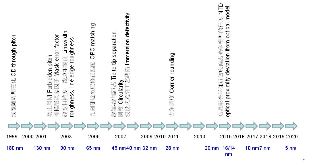
In Figure 2, the technology nodes where the above mentioned inventions are used is displayed. For example, the quadrupole illumination mode is first used in the 90 nm logic technology node, the polarization in the illumination is first used in the 45 nm technology node, the opaque Molybdenum-Silicide on glass (OMOG) mask was first used in the 22 nm technology node, etc. In the figure, there are some technology that are superseded by more advanced version, such as, the rule-based optical proximity correction (OPC) has been used in 0.25 and 0.18 μm technologies, but was replaced by more advanced model-based OPC starting 0.13 μm technologies. The wafer CDU tuning within dose mapping methodology (DoMa) that are used in 0.13 μm technology was replaced by more advanced dose mapping and correction within both exposure shot and wafer version starting the 90 nm technology node. There is also some special technology that have only been used in several technology modes. One of them is the alternating phase shifting mask (Alt-PSM) that has been used for 3 technology nodes.
Figure 1.
Invented tools, materials, devices, or methods/methodologies for photolithography. Figure 2.
Invented tools, materials, devices, or methods/methodologies for photolithography and the technology nodes where they are used. 3. Major Process Parameters by Logic Technology Nodes
The most common parameters that characterizes photolithography process are as follows:
• Exposure latitude/Depth of focus (EL/DoF)
• Photoresist etch resistance/thickness/thickness uniformity
• Photoresist cross section profile
• Across chip/across wafer linewidth variation (ACLV/AWLV)
• Pattern corner rounding
Over the years, more parameters have been added:
• CD through pitch (~1999, 180 nm node)
• Forbidden pitch (2002, 110 nm node)
• Mask error factor (2002, 110 nm node)
• Linewidth roughness, line edge roughness (~2003, 90 nm node)
• OPC matching (~2005, 65 nm node)
• Tip to tip separation (2007, 45 nm node)
• Circularity (~2007, 45 nm node)
• Immersion defectivity (2007, 45 nm node)
• Corner rounding (2011, 28 nm node)
• NTD optical proximity deviation from optical model (2015, 14 nm node)
The addition is a result of increasingly higher requirement for process window and linewidth uniformity and the need to be able to fully model and utilize the process. For example, the CD through pitch is introduced due to increasingly small k1 value under which only isolated to dense linewidth bias cannot describe the optical proximity effect well. When the proximity effect becomes more pronounced, there is certain pitch range can become very difficult to print. The “forbidden pitch” was used to describe this effect starting around 110 nm process nodes. Although the so-called “forbidden pitch” is not really avoided by design until nodes below 28 nm, the device patterns designed within such pitch range does have degraded linewidth uniformity performance. The mask error factor (MEF) has become a severe issue at the 110 nm technology node. In the years of 65 nm node, the 193 nm dry process has reached a limit, the optical proximity effect has become challenging, and the understanding of 193 nm photoresist has become mature
[8,9 ], there emerges a need to match OPC from different photoresist and exposure tools to speed up process transfer and expansion. In the years of the 45 nm technology node, the tip-to-tip separation has become a limitation for the chip design, the 193 nm immersion photoresist can print a tip-to-tip distance around 60-70 nm, which is close to the CD of 80-90 nm. At more advanced technology nodes, the tip-to-tip distance will not improve much, the limit of the parameter is 55 nm for positive toned developing (PTD) and 60 nm for negative toned developing (NTD). However, at the most advanced technology nodes 7 nm, the metal CD is around 20 nm through double patterning, significantly smaller than the above tip-to-tip distance (55-60 nm) that the 193 nm immersion process can support.
Circularity is a parameter that measures the pattern fidelity of contact/via hole printing. When the overlay becomes critical, it can affect total yield. However, the circularity is just like linewidth roughness (LWR) or line edge roughness (LER), which is very difficult to improve. Usually the limit of LWR is 4 nm (3-sigma), which is a reflection of photoresist granularity and image contrast and can only be realized using dipole illumination and low activation energy photoresist. For the contact layer, the only illumination that is practical is annular. A sensible LWR range is around 6-8 nm. In case of overlay issue, it would be better to improve OPC accuracy and CDU rather than focusing on the circularity improvement.
Immersion defectivity has emerged with the introduction of 193 nm water immersion photolithographic process. Although it seems to mostly attribute to the hardware improvement, the photoresist has also been required to leach less into the immersion water.
Corner rounding is basically ignored before the introduction of 32/28 nm technology nodes. The corner rounding radius for the 248 nm process is around 100-160 nm, and 35-45 nm for the 193 nm immersion process. At the 32/28 nm technology nodes, the corner rounding radius has approached the CD numbers, which are 45-50 nm for 193 nm immersion layers and 145-160 nm for the 248 nm layers. Small corner rounding radius can help to shrink chip area.
NTD process has been introduced at 14 nm MEOL and BEOL layers, it has the advantages of superior contrast and MEF performance for the semi-dense and isolated pitches. And even for the dense pitch, its performance has been improving to the minimally acceptable level. NTD process, however is not friendly to the OPC modeling. Its linewidth can differ from the traditional PTD model by 15-20 nm at semi-dense and isolated pitches. Until very recently, it has been understood
[10]. The NTD process, similar to that of most negative toned photoresist, relies on some level of saturation in the photochemical reaction. The saturation process is non-linear and will deviate from the original linear representation of the aerial image from the photoacid diffusion-reaction process. For a successful process development, the similarity of a NTD process to the linear optical model is important to cycle time and CDU.
4. Major Process Window Values by Logic Technology Nodes
Shown in Figures 4(a) and 4(b) is a table of important process window parameter values for various technology nodes from 0.25 μm to 7 nm. The parameters list here is the exposure latitude (EL) and mask error factor (MEF). The numbers here are simulated with typical process parameters, such as the mask type (binary, 6% attenuated phase shifting, OMOG), photoresist thickness, pitch, linewidth, wavelength (248 nm, 193 nm, 193 nm immersion), photoacid diffusion length (from 70 to 5 nm), the illumination condition (conventional, annular, cross quadrupole, weak dipole, strong dipole, SMO). The figures show that the illumination condition evolves from the conventional and annular used by 0.25 μm through 65 nm, to dipole and quadrupole used to 45 nm through 22 nm, and to pixelated (source-mask optimized, SMO’ed) used by 20 nm through 7 nm. The evolution of the illumination condition reflects the need to print ever smaller pitch. At the same time, the wavelength has also been reduced from 248 nm to about 134.7 nm, though not much. There is another important parameter that shrinks aggressively: the photoacid diffusion length. It has been reduced from the 70 nm at the 0.25 μm technology node to about 5 nm at 22 nm and below nodes, a 14 time shrink. This has been mostly overlooked by many lithographers. But the magnitude of the shrink has demonstrated itself to be at the same level to that of the linewidth (around 12.5 X from 250 nm to 20 nm).
Figure 3.
The year and technology node when some photolithographic process parameters have been added. Figure 4.
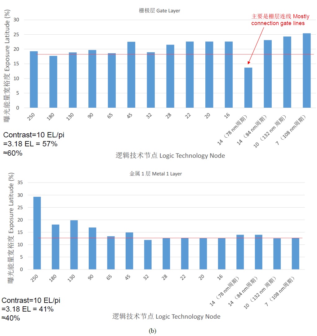
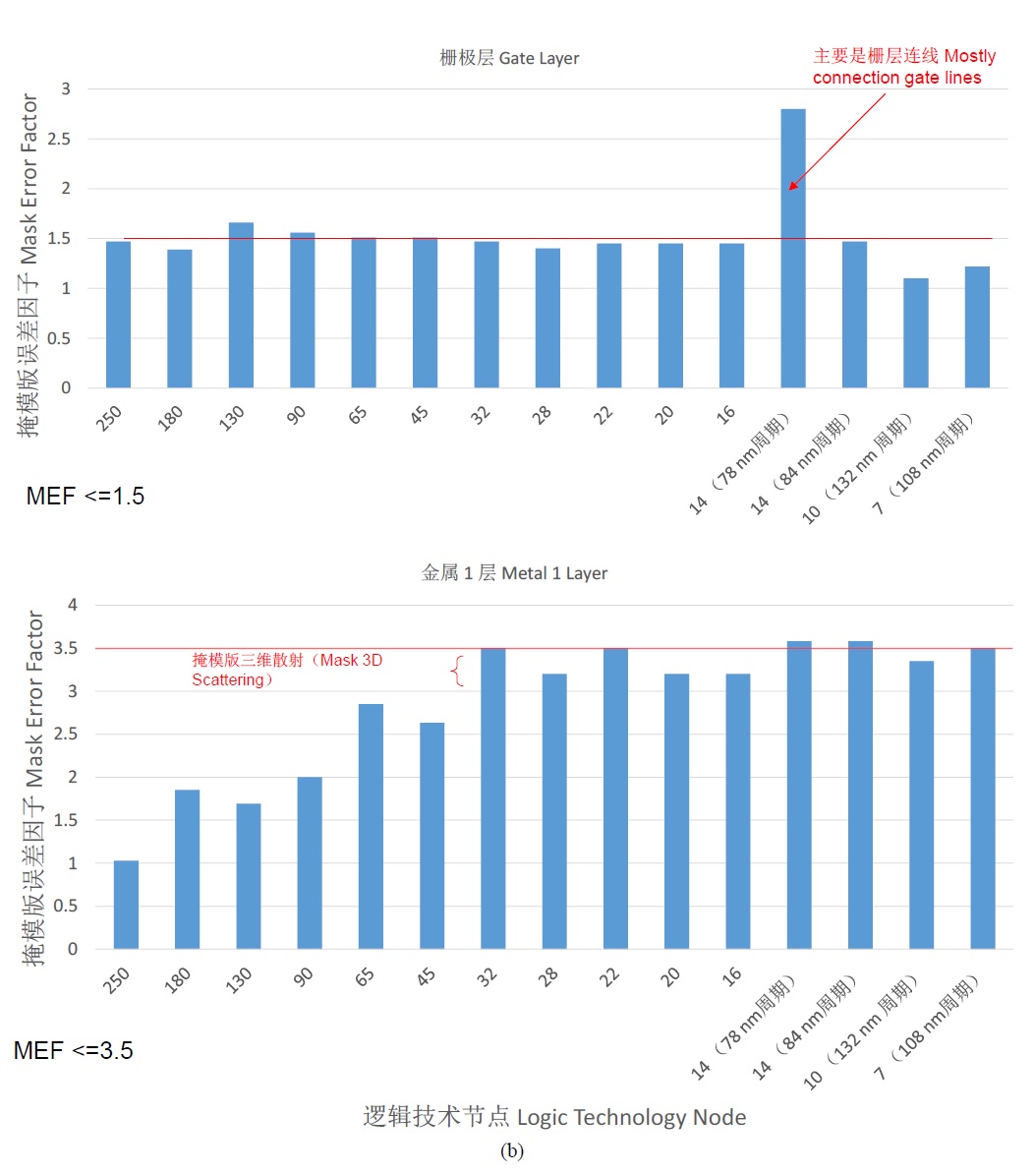
(a) A simulated EL and MEF numbers for the Gate and Metal layers for typical technology nodes from 0.25 μm to the 7 nm. (b) Same to (a) with categorization. Shown in Figures 5(a) and 5(b) are exposure latitude numbers for the gate and metal 1 layers at the minimum pitch for the technology nodes ranging from 0.25 μm to 7 nm. The data indicates that the exposure latitude for the gate layer is basically constant, at 18% or above, with the exception of 78 nm pitch at 14 nm node (where the gate line is mostly connection wire). The metal layer, however, has an exposure latitude going from an initial high number of 28% at 0.25 μm technology node and gradually decreasing and remain constant at 65 nm nodes. The constant is around 13%. The 18% and 13% numbers are a result of linewidth uniformity requirement. To make this more intuitive, we correlate the exposure latitude numbers with imaging contrast.
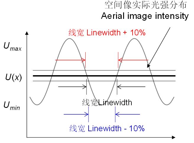
Described in Figure 6 is a schematic illustrating the definition of exposure latitude. At the minimum pitch, the aerial image of a dense line/space is a sinusoidal function due to interference of two light beams (the zeroth order and the first order). Noticing the definition of the image contrast, defined in Equation (1), the aerial image intensity U(x) can be written in the form shown in Equation (2), as follows,

(1)

(2)
where Umax and Umin represents the maximum and minimum intensity, respectively, p represents pitch and U0 is a proportional constant.
Figure 5.
(a) A simulated EL for the Gate layer as a function of technology nodes from 0.25 μm to the 7 nm. (b) A simulated EL for the Metal layer as a function of technology nodes from 0.25 μm to the 7 nm. The definition of the exposure latitude EL is the ratio of the exposure energy spread ΔE to the exposure energy to linewidth target E due to +/- 10% linewidth variation, defined in Equation (3), as follows,

(3)

. (4)
According to Equation (2), Equation (3) can be written as Equation (4), where L and ΔL represent linewidth and linewidth variation range, which is 0.1L. When the linewidth L equals to the 1/2 of the pitch p, Equation (4) can be simplified as follows,

. (5)
According to Equation (5), the imaging contrast is roughly 3.2 EL. Therefore the 18% and 13% exposure latitude for the dense pitches are equivalent to image contrast numbers of 57.6% and 41.6%, respectively, or roughly 60% and 40%.
Figure 6.
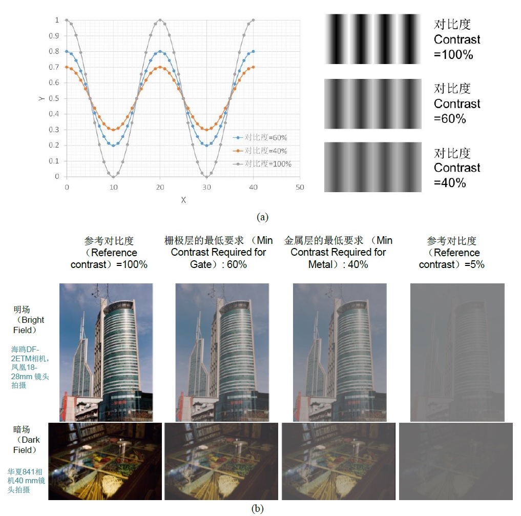
Schematic that illustrates the definition of exposure latitude. Shown in Figures 7(a) are simulated 1D line/space grey scale images at three level of image contrast: 100%, 60%, and 40%, respectively. The images indicate that the needed gate layer contrast is visibly better than that of the metal layer. Shown in Figure 7(b) are two photos under bright field and dark field conditions showing the same three level of image contrast plus a 5% contrast for comparison. The 40% contrast images seems to reach a comfortable-uncomfortable limit while the 60% contrast images seems to reveal all image details with just a casual glance (my feeling, laugh). These are the analogy to the everyday photography.
Figure 7.
(a) Plots of 1D line/space images showing 3 level of image contrasts: 100%, 60%, and 40%, respectively. (b) Photos of both bright field and dark field types at 4 level of image contrasts: 100%, 60%, 40%, and 5%, respectively. The other important parameter of the process window we will show is the mask error factor (MEF), or the so-called mask error enhancement factor (MEEF). If the exposure latitude is related to image contrast, which is related to the across wafer linewidth uniformity, the mask error factor will be related to the within exposure shot linewidth uniformity.
Figure 8.
(a) A simulated MEF for the Gate layer as a function of technology nodes from 0.25 μm to the 7 nm. (b) A simulated MEF for the Metal layer as a function of technology nodes from 0.25 μm to the 7 nm. Figures 8(a) and 8(b) show mask error factor numbers for the gate and metal 1 layers at the minimum pitch for the technology nodes ranging from 0.25 μm to 7 nm. As we can see, the MEF for the gate layer remains pretty much as 1.5 or lower with the exception of 78 nm pitch at 14 nm node (where the gate line is mostly connection wire). And the MEF for the metal layer starts at an initial low number of 1 at the 0.25 μm technology node and gradually increasing and remain constant at 32 nm nodes. The constant is around 3.5. A small jump at the 32 nm technology node is due to the mask 3D scattering effect, which adds about 0.7 on top of the 45 nm MEF values. The 3.5 versus 1.5 indicates that the metal linewidth uniformity can have a relaxed tolerance compared to the gate.
5. Linewidth Uniformity Requirement by Logic Technology Nodes
As a continuation from the last section, in this section we summarize our study of linewidth uniformity requirement for different technology nodes. We starts from the ITRS (International Technology Roadmap for Semiconductors) publication on the recommended numbers
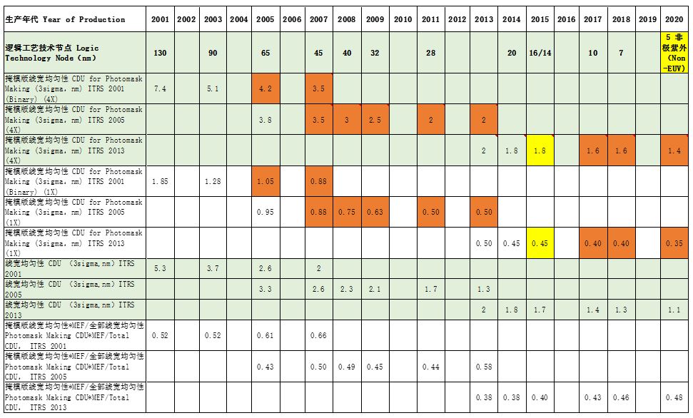
[11,12,13 ]. Shown in Table 1 is a list of ITRS pitch/CD number and CD uniformity (CDU) requirement for technology nodes from 130 nm to 5 nm. We reference three ITRS publication versions: the ITRS 2001, 2005, and 2013. In case of any difference between the versions, we pick the more recent numbers. In the last two lines of the Table 1, we calculate the ratios of the CDU to both the gate physical CD and gate half pitch.
The calculation reveals the following:
(1) The gate linewidth control tolerance relative to its physical linewidth is nearly constant, about +/-10%.
(2) The gate linewidth control tolerance relative to gate half pitch increases as the diffraction limit is approached (20 nm and 16/14 nm nodes) from +/- 3% to +/- 4%, and to +/-5% as double patterning methods are used (10 nm, 7 nm, and 5 nm nodes).
The above result reflects that the key to the gate linewidth uniformity control is to support CMOS transistor performance requirement which follows a fixed linewidth uniformity requirement during the course of design rule shrink. And the physical linewidth becomes closer to the half pitch.
Accordingly, the mask linewidth uniformity has also followed a trend of reduction as the technology nodes advance. Shown in Table 2 is a list of mask linewidth uniformity specification originally from the ITRS 2001, 2005, and 2013, and adjusted with the practical mask making capabilities for the gate layer. The top 3 lines below the line of technology nodes are 4X specifications, and the next 3 lower lines are 1X specifications (4X number divided by 4), and the next lower 3 lines are wafer total CDU numbers (also from Table 1), the last 3 lines are the ratio of mask linewidth uniformity multiplied by MEF numbers to the total CDU numbers, which shows a trend going from 0.52 at the 130 nm node to a low 0.38 at the 20 nm node and rises to a 0.48 at the 5 nm node. This number is nearly constant.
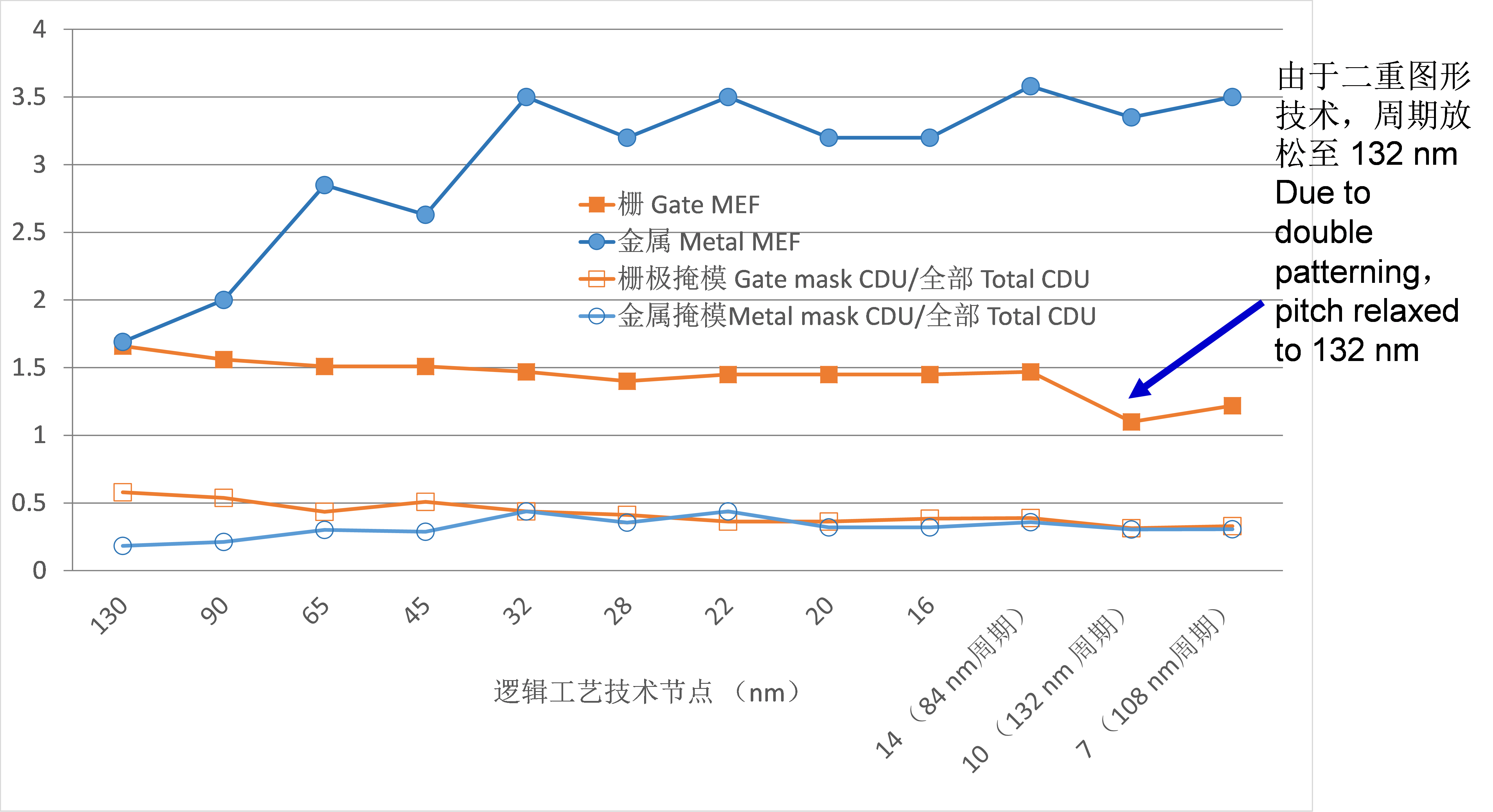
Figures 9 shows the ratio of mask linewidth uniformity for both the gate and metal layers multiplied by MEF to the total wafer CDU as a function of technology nodes from 130nm to the 5 nm. As discussed before, the gate MEF is nearly constant at 1.5, the ratio of mask CDU contribution (mask CDU multiplied by MEF) to the total wafer CDU is also nearly constant at 0.4-0.5. This means that the mask contribution to the total wafer CDU for the gate is kept at about 0.4-0.5. In the case of the metal layer, however, the situation is different. Starting from 130 nm through 45 nm, the contribution from the mask is quite low, around 0.20 to about 0.30, from 32 nm node and newer, the contribution from the mask is similar to that of the gate layer, around 0.4-0.5. This is because a jump in MEF about 0.70 due to the mask 3D scattering effect.
Table 1.
CDU requirement for the gate layer at major logic technology nodes. Table 2.
CDU requirement for photomasks at major logic technology nodes. Figure 9.
Ratio of mask linewidth uniformity for both the gate and metal layers multiplied by MEF to the total wafer CDU as a function of technology nodes from 130nm to the 5 nm. And the MEF values for both the gate and metal layers multiplied by MEF to the total wafer CDU as a function of technology nodes from 130nm to the 5 nm.