Authors: Wenzhan Zhou, Hung-Wen Chao, Yu Zhang et al.
Institution:Shanghai Huali Integrated Circuit Corp, China
Keywords:Design for Manufacturing (DFM);Design Friendly Manufacturing;EUV Lithography;Source Mask Optimization (SMO);Design Technology Co-optimization (DTCO);Process Window;Process Variation
doi:10.33079/jomm.20030101
Abstract:
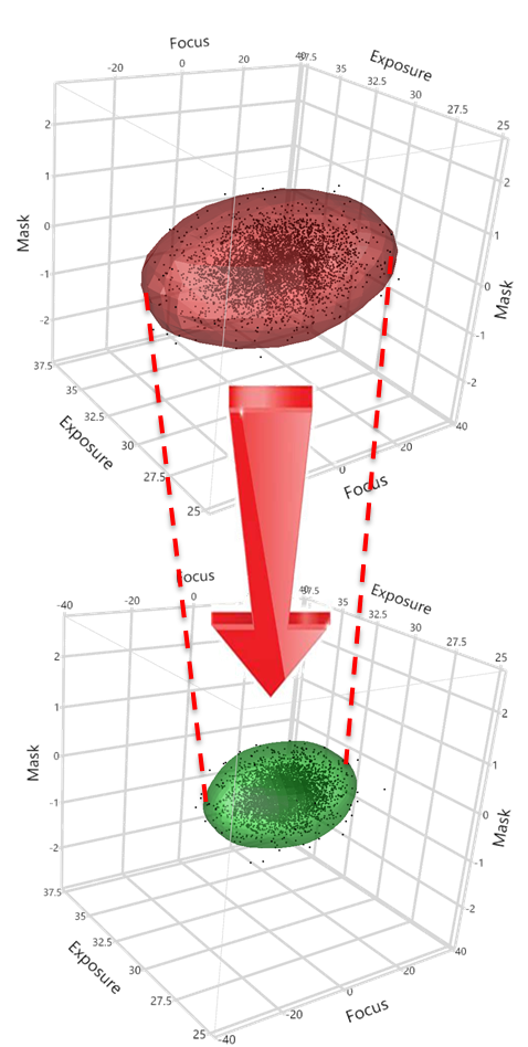
As the IC manufacturing enter sub 20nm tech nodes, DFM become more and more important to make sure more stable yield and lower cost. However, by introducing newly designed hardware (1980i etc.) pro...
Authors: Wei Zhang, Jun Xu, Sicong Wang et al.
Institution:Yangtze Memory Technologies Co., Ltd., Wuhan
Keywords:3D NAND;Metrology;Semiconductor;HAR;Process Control
doi:10.33079/jomm.20030102
Abstract:
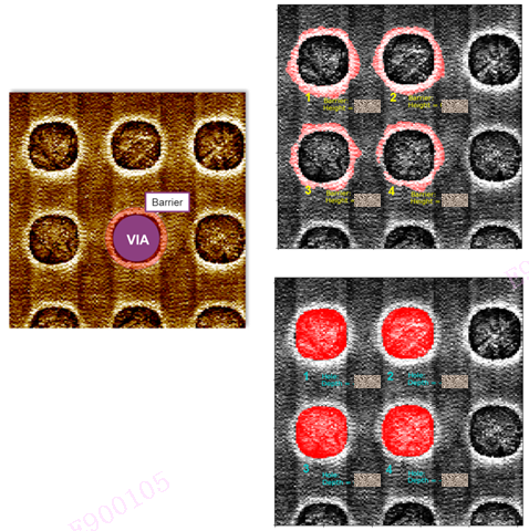
3D NAND technical development and manufacturing face many challenges to scale down their devices, and metrology stands out as much more difficult at each turn. Unlike planar NAND, 3D NAND has a thr...
Authors: Yushu Yang, Yanli Li, Qiang Wu et al.
Institution:Shanghai IC R&D Center, 497, Gaosi Road, Zhangjiang Hi, -, Tech Park, Shanghai
Keywords:5 nm Logic Process;EUV;metal gate cut;SAC;BAC;self-aligned LELE
doi:10.33079/jomm.20030103
Abstract:
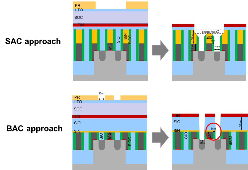
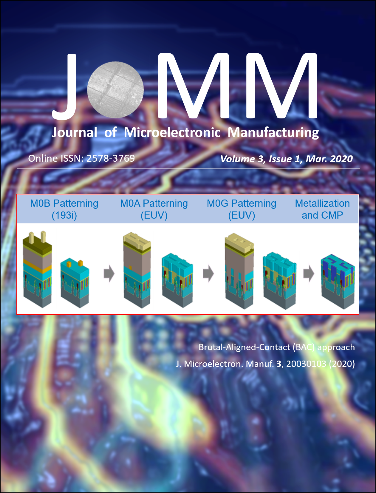
5 nm logic process is the current leading-edge technology which is under development in world-wide leading foundries. In a typical 5 nm logic process, the Fin pitch is 22~27 nm, the contact-poly pi...
Authors: Liang Zhu, Barry Ma, Lin Shen et al.
Institution:Synopsys Inc., 1027 ChangNing Road, Shanghai, China, 200050
Keywords:Assist Feature;Inverse Lithography Technology;Low K1 Lithography;Machine Learning
doi:10.33079/jomm.20030104
Abstract:
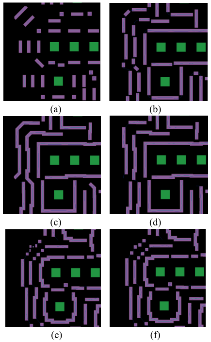
Sub-resolution assist features have been widely recognized in lithography patterning. In general, the insertion of assist features in optically adjacent space around main designed features, will ch...
Authors: Yu Ding, Yongfeng Cao, Xin Luo et al.
Institution:Shanghai Integrated Circuit Research and Development Center, No, ., 497, Gaosi Road, Pudong New Area, Shanghai
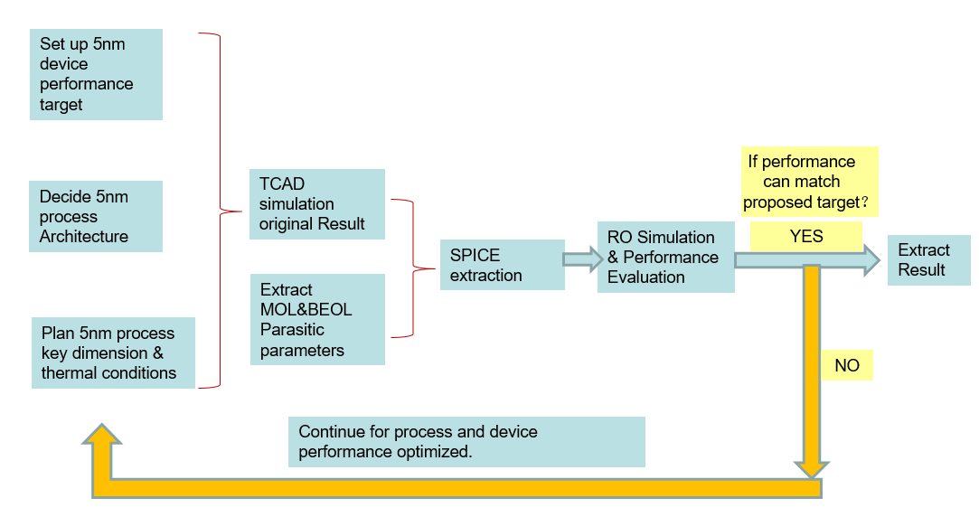
Keywords:5nm FinFET;brief process flow;key dimensions;simulated device DC/AC performance;RO PPA performance
doi:10.33079/jomm.20030105
Abstract:
With the continuous scaling in conventional CMOS technologies, the planar MOSFET device is limited by the severe short-channel-effect (SCE), Multi-gate FETs (MuG-FET) such as FinFETs and Nanowire, N...
Authors: Litho World
Keywords:IC Industry;Material lndustry
doi:10.33079/jomm.20030106
Abstract:
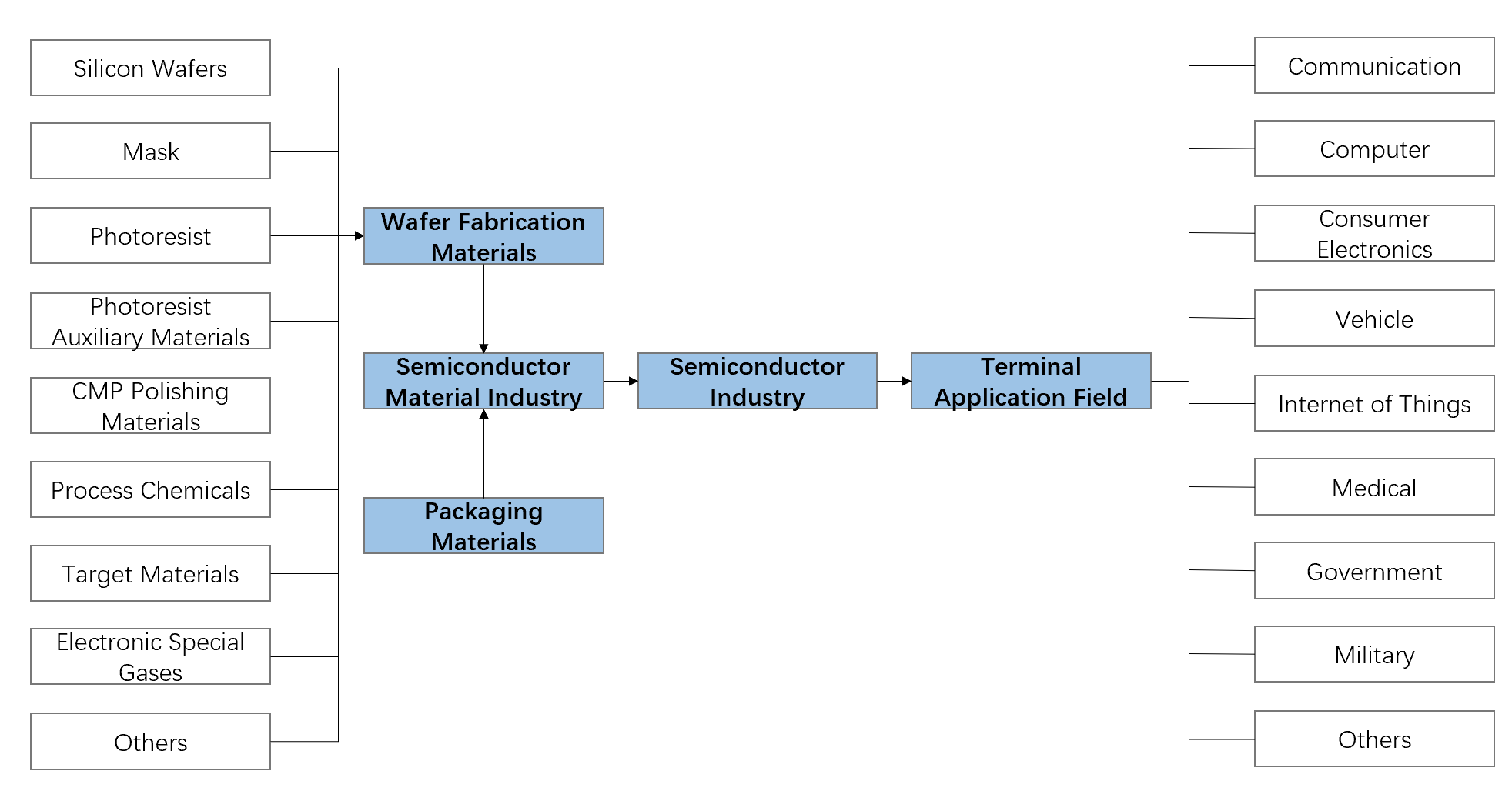
China's IC industry has been flourishing in recent years, huge market demand together with government investments are the major driving forces for this development. The status and development momen...