Research Article Archive Versions 1 Vol 3 (1) : 20030105 2020
Download
A Device Design for 5 nm Logic FinFET Technology
: 2019 - 11 - 29
: 2020 - 03 - 30
2530 91 0
Abstract & Keywords
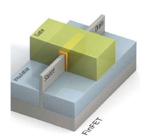
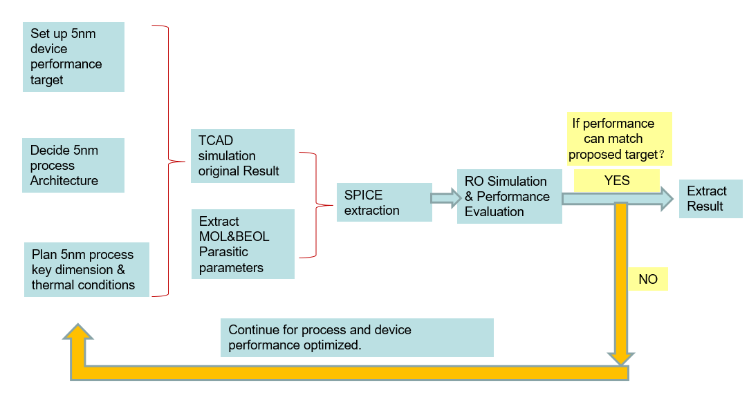
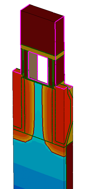
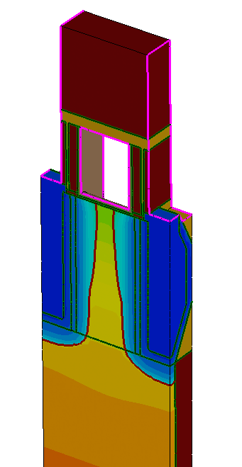
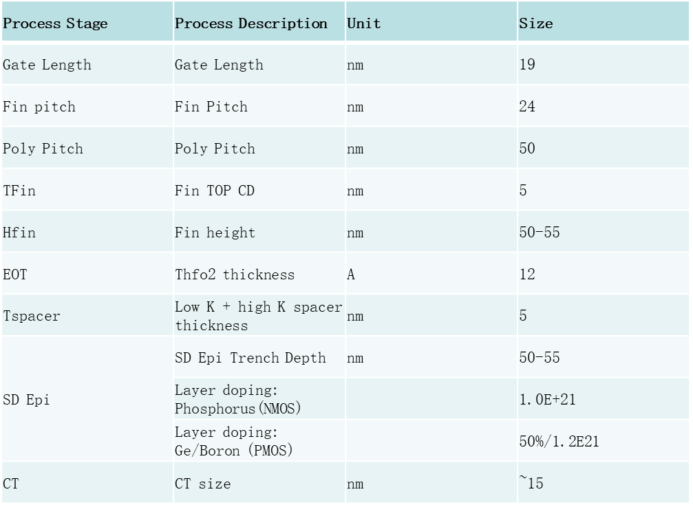
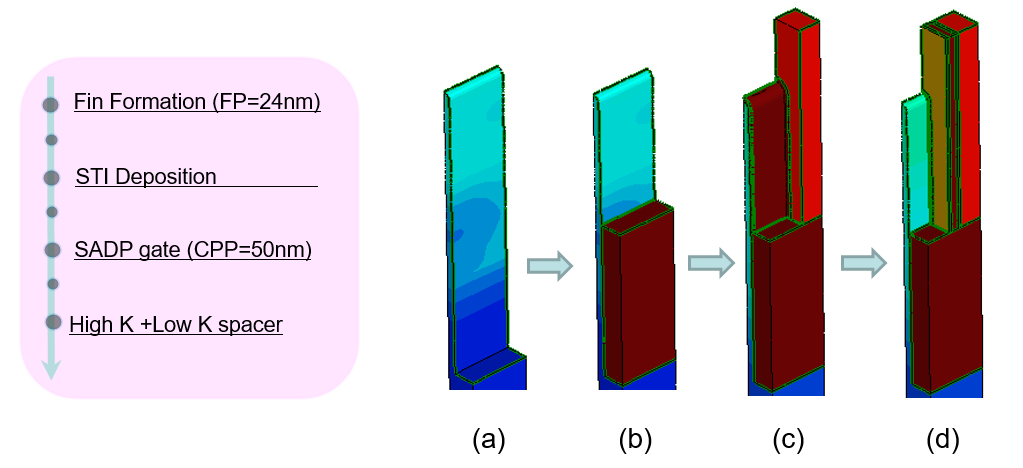
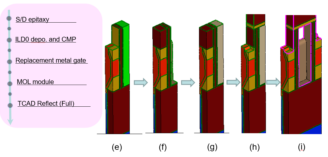
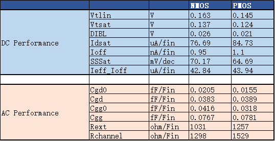
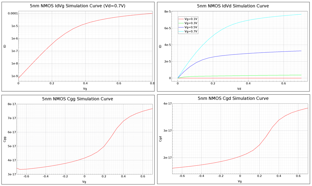
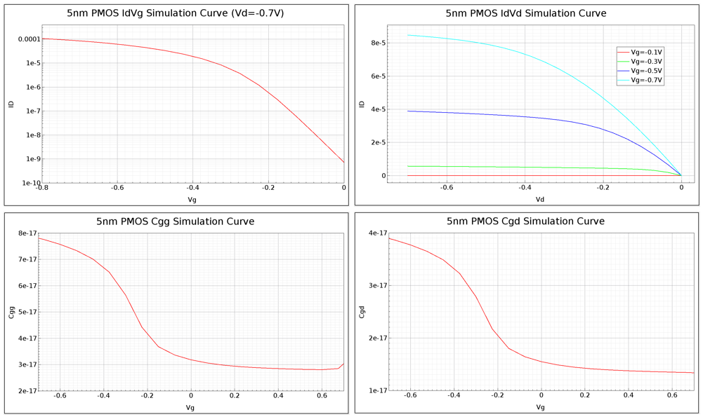
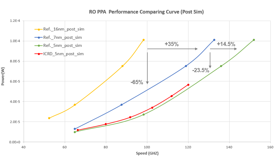
Abstract: With the continuous scaling in conventional CMOS technologies, the planar MOSFET device is limited by the severe short-channel-effect (SCE), Multi-gate FETs (MuG-FET) such as FinFETs and Nanowire, Nanosheet devices have emerged as the most promising candidates to extend the CMOS scaling beyond sub-22 nm node. The multi-gate structure has better short channel behaviors due to enhanced control from the multiple gates. Due to the relatively more mature process and rich learning of the device physics, the FinFET is still extended to 5 nm technology node. In this paper, we proposed a 5 nm FINFET device, which is based on typical 5 nm logic design rules. To achieve the challenging device performance target, which is around 15% speed gain or 25% power reduction against the 7 nm device, we have performed an optimization on the process parameters and iterate through device simulation with the consideration of current process capability. Based on our preferred device architecture, we provide our brief process flow, key dimensions, and simulated device DC/AC performance, like Vt, Idsat, SS, DIBL and parasitic parameters. As a part of the final evaluation, RO simulation result has been checked, which demonstrates that the Performance Per Area (PPA) is close to industry reference 5 nm performance.
Keywords: 5nm FinFET; brief process flow; key dimensions; simulated device DC/AC performance; RO PPA performance
1.   Introduction
As MOSFET scales down, the conventional planar transistor architectures have already reached the fundamental material and process technology limits. Besides, as the size decreases, the device will suffer from the short channel effects (SCE), which result in the severe leakage problem and mobility degradation, and hence the effective drive current will drop. The threshold voltage (Vt) will also roll-off. Thus, a high channel doping to control the leakage current is required. However, it has major disadvantages of lower carrier mobility, high tunneling effect, degradation in subthreshold performance, and larger parasitic capacitance.


Figure 1.   Schematic of FINFET Structure.
Therefore, the development of small devices with high performance becomes more challenging. Innovative three-dimensional structures such as double-, triple-, fin-typed, nanosheet, and nanowire field-effect transistors (FET) have been of great interests. Fin-typed FET (FinFET) is one of the most promising device structures to address short-channel effects and leakage issues in the deeply nano-scale transistor. FinFET structure mitigates these problems at low channel doping conditions, which also minimizes variations of the Vt, reduces subthreshold leakage current, keeps high carrier mobility, and enhances the drive current. Thus the FinFET structure can be scaled down to 22 nm and beyond.
In this paper, we have developed a 5 nm FINFET structure with TCAD simulation support. In details, we propose our development procedure, introduce our brief process flow, present key dimensions and simulated device performance.
2.   Simulation Approach
2.1.   Device Development Procedure
Firstly, we introduce our 5 nm development procedure shown in Figure 2, as follows.


Figure 2.   5 nm device development procedure.
In the beginning, we set up our device targets through material path-finding study, and then determine the architecture and process conditions. We perform the TCAD simulation with these conditions ready and get the initial result. Next combine with Middle-Of-the-Line (MOL) & Back-End-Of-The-Line (BEOL) extracted parasitic parameters, we extract the SPICE model parameters, and take the result into Ring Oscillator (RO) simulation, if the Performance Per Area (PPA) can meet our initial target, then we extract our device data and curves as a result; if not, then as a learning circle, we will continue to optimize our simulation conditions.
2.2.   Device structure
Figure 3 illustrates the device architecture of the simulated FinFET and cross-section view of the device doping profile.

(a)


(b)

Figure 3.   (a) NFET; (b) PFET.
In this simulation, a Fin pitch of 24 nm, a Poly pitch of 50 nm, and a total gate length (LG) of 19 nm have been adopted. We set the top fin-width (Tfin) = 5 nm and the fin-height (FH) equal to 50-55 nm as a standard device; (SiO2+HfO2) were considered as the gate oxide and (low K+ high K Si3N4) as spacer material. Fixed total spacer length (LSP) of 5 nm was used. The doping concentrations were Phosphorus 1.0E21 for NFET and Boron 1.2E21 for PFET respectively in the source/drain (S/D) region. Around 15 nm contact (CT) dimension was applied. The key dimension of different parameters for the simulated device is listed in Table 1.


Table 1.   Device parameters used in the simulation.
2.3.   Simulation Process Flow
The brief process flow used in our 5 nm FinFET device simulation was shown in Figures 4.1 and 4.2. First, we define the fin profile, and the critical dimension of fin width has been shown in Table I. Followed by STI deposition, and then the poly gate formation, in which the gate region is wrapped around the three sides of the fin channel. The gate oxide is formed under the gate. By extending gate control to three sides of the fin, it will allow the relatively shorter gate length. Next, S/D offset spacers and spacers are formed along the sidewalls of the gate and fin. The sidewall spacers on the fins are subsequently removed to expose the fin to grow raised source and drain using selective epitaxy.


Figure 4.1.   General process flow of a FINFET device simulation with process steps (a) through (d).
Source and drain extensions are formed by epitaxy, the raised source and drain structure help to reduce the parasitic resistance associated with thin fins. Next, ILD film deposition and planarization, and then the gate dielectric is grown and poly gate is replaced by metal gate. Then, contact connection has been defined. Finally, before the Sentaurus S-device simulation, we should do structure reflect (To save simulation time, we just do half side structure simulation in the S-Process).


Figure 4.2.   General process flow of a FINFET device simulation with process steps (e) through (i).
2.4.   Simulation Result
In this section, we present our simulated device DC/AC performance in Table 2, which indicates that the Drain Induced Barrier Lowering (DIBL) is around ~25 mV and Subthreshold Slope (SS) is ~65-70 mV/decade, which is comparable with published reference performance and demonstrate that our short channel effect has been controlled well.
The parasitic parameters, like Cgd0 is around 0.0205 fF/Fin and 0.0155 fF/Fin for NFET and PFET respectively; Both Rext and Rchannel are also acceptable, NFET has around ~1031ohm/Fin Rext and ~1298ohm/Fin Rchannel, PFET has around ~1257ohm/Fin Rext and ~1529ohm/Fin Rchannel, further improvement is ongoing.


Table 2.   The simulated device DC/AC performance result.
Figure 5 and Figure 6 show the IdVd, IdVg, Cgg, Cgd curves for the NFET and PFET, respectively.


Figure 5.   Characteristic curves for the NFET Device from simulation.


Figure 6.   Characteristic curves for the PFET Device from simulation.
Finally, to have a comprehensive understanding, we make the Ring Oscillator (RO) simulation. In Figure 7, it seems our 5 nm RO PPA performance is close to industry reference 5 nm performance. (Industry reference is published with 35% speed gain and 65% power reduction from 14 nm to 7 nm and 14.5% speed gain and 23.5% power reduction from 7 nm to 5 nm, respectively).


Figure 7.   RO PPA performance comparison.
3.   Conclusion
In this paper, we have performed a simulation to study a typical 5 nm FinFET device structure and performance. The result indicates that our device performance is comparable with published reference performance and the short channel effect is controlled well; our ring oscillator simulation demonstrates that the PPA is also close to industry reference 5 nm performance. We believe that the FinFET device still has the ability to extend to 5 nm technology node with continued performance gain.
Acknowledgments
The authors would like to thank the management team and all our team members in Shanghai ICRD center.
[1] Colinge, Jean-Pierre. "The SOI MOSFET: From single gate to multigate." FinFETs and Other Multi-Gate Transistors. Springer, Boston, MA, 2008. 1-48 (2008).
[2] Xiong, Weize Wade, “Multigate MOSFET technology." FinFETs and Other Multi-Gate Transistors, Springer, Boston, MA, 2008. 49-111 (2008).
[3] Kurniawan, Erry Dwi, et al. "Effect of fin shape of tapered FinFETs on the device performance in 5-nm node CMOS technology." Microelectronics Reliability 83 (2018): 254-259 (2018).
[4] Lin, Chung-Hsun, et al. "Non-planar device architecture for 15nm node: FinFET or trigate?" 2010 IEEE International SOI Conference (SOI). IEEE, 2010 (2010).
[5] Ota, Hiroyuki, et al. "Fully coupled 3-D device simulation of negative capacitance FinFETs for sub 10 nm integration." 2016 IEEE International Electron Devices Meeting (IEDM). IEEE, 2016 (2016).
Article and author information
Yu Ding
dingyu@icrd.com.cn
Yongfeng Cao
Xin Luo
Enming Shang
Shaojian Hu
Shoumian Chen
Yuhang Zhao
Publication records
Published: March 30, 2020 (Versions1
References
Journal of Microelectronic Manufacturing