Authors: Lei Qu, Rui Chen, Xiaoting Li et al.
Institution:North China University of Technology, China
Keywords:thin film deposition;atomic layer deposition;growth model;prediction model;simulation method
doi:10.33079/jomm.19020204
Abstract:
Thin film deposition is one of the most important processes in IC manufacturing. In this paper, several typical models and numerical simulation methods for thin film deposition and atomic layer dep...
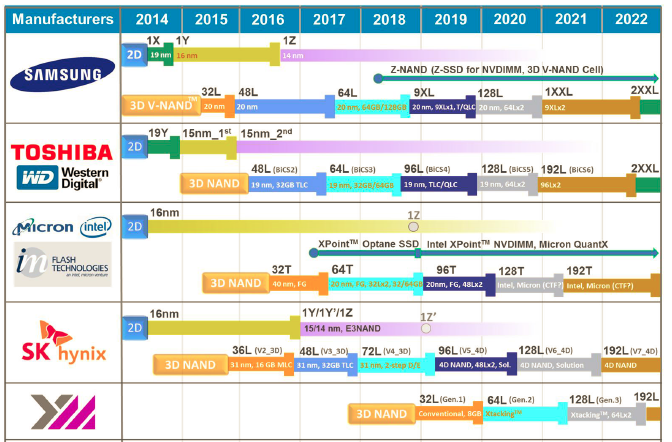
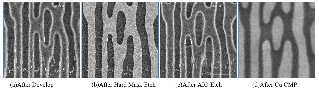
Authors: Yu Zhang, Abhishek Vikram, Ming Tian et al.
Institution:Shanghai Huali Microelectronics Corp, ., Pudong District, Shanghai
Keywords:Die-to-database Pattern Monitor;After Develop Inspection (ADI);After Etch Inspection (AEI);SEM Review;CDSEM;pattern centric;pattern monitor
doi:10.33079/jomm.19020203
Abstract:
Normally the optical wafer inspection tools are used for advanced process control in high volume manufacturing of semiconductor devices. The SEM Review is done for limited sample of inspection defe...
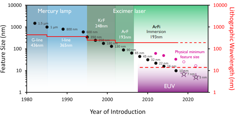
Authors: Nan Fu, Yanxiang Liu, Xiaolong Ma et al.
Institution:HiSilicon Technologies Co, ., Ltd, Shanghai
Keywords:EUV lithography;EUV review;mask 3D;line edge roughness;EUV light source
doi:10.33079/jomm.19020202
Abstract:
Although several years delayed than its initial plan, extreme UV lithography (EUVL) with 13.5nm wavelength has been finally implemented into high volume manufacture (HVM) of mainstream semiconducto...
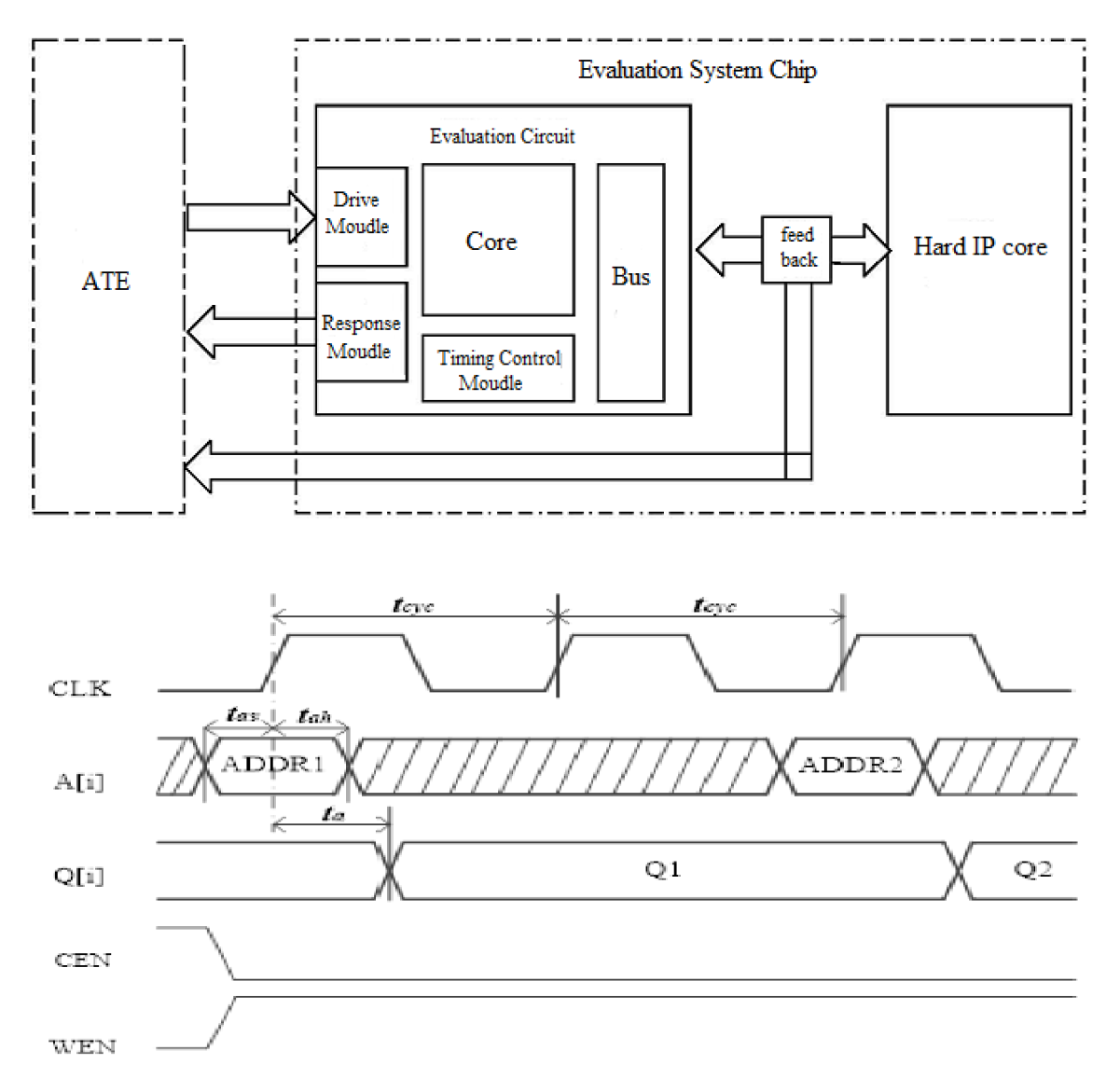
Authors: Kun Yu, Hua Wang
Institution:Sino IC Technology Co, ., Ltd, ., Shanghai
Keywords:hard IP core;system on chip (SOC);testing technology;evaluation circuit;memory;automatic test equipment (ATE)
doi:10.33079/jomm.19020201
Abstract:
Based on the analysis of the existing hard IP core testing technology, the hard IP core nondestructive testing technology was studied, according to the verification requirements of a large number o...