Research Article Archive Versions 2 Vol 2 (2) : 19020204 2019
Download
Development and Prospect of Process Models and Simulation Methods for Atomic Layer Deposition
: 2019 - 05 - 23
: 2019 - 06 - 26
2574 64 0
Abstract & Keywords
Abstract: Thin film deposition is one of the most important processes in IC manufacturing. In this paper, several typical models and numerical simulation methods for thin film deposition and atomic layer deposition are introduced. Several modeling methods based on the characteristics of atomic layer deposition are introduced, it includes geometric method, cellular automata and multi-scale simulation. The principle of each model and simulation method is explained, and their advantages and disadvantages are analyzed. Finally, the development direction of thin film deposition and atomic layer deposition modeling is prospected, and some modeling ideas are also provided.
Keywords: thin film deposition; atomic layer deposition; growth model; prediction model; simulation method
1.   Introduction
In the integrated circuit manufacturing process, the deposition technology is among the most popular technologies. The purpose of the thin film deposition is to grow thin films of different thickness and different materials onto the wafer surface by physical or chemical methods to prepare for the subsequent photolithography and etch and ion implantation process [1, 2]. Deposition can be divided into two categories according to principle: physical process and chemical process. Physical processes can be divided into evaporation, sputtering and other technologies. The chemical process can be divided into chemical vapor deposition (CVD), plasma enhanced CVD (PECVD), atomic layer deposition (ALD) and other techniques.
With the continuous development of process technology nodes, the minimum feature size is further reduced, and the performance of thin film deposition technology is becoming more and more important in integrated circuit manufacturing. Especially for the application of atomic layer deposition technology, because it has more fine film thickness scale (atomic level) and safer temperature (300℃-500℃) [1, 3] than other thin film growth technology, it gradually becomes 14 nm. One of the technologies relied upon by the 7nm and the following process nodes. However, the technical challenges brought by the size reduction also increase, and the modeling can be used to better analyze the performance of the film, predict the surface profile after the reaction, and help reduce defects, therefore the modeling of the film growth process is also carried out. The PVD and CVD process have to predict reaction after the outline of the model, and the growth rate and substrate contact, and so on and so forth ideal modeling method, the steps for ALD technology, at present results mainly concentrated in the thin film nucleation and growth of nuclear, and the prediction model for more tube type special graphic modeling, such as growth rate and the main research problems, such as low precision model. Therefore, the establishment of models suitable for ALD process requirements has become the top priority in solving the problem. However, with the improvement of computer operation ability and the improvement of model synthesis degree to deal with problems, the model details are more real and the fitting degree with real data is also improving.
Several conventional models and numerical simulation methods for simulating film growth are introduced in this paper. Their characteristics, application mode, advantages and disadvantages are briefly introduced. Finally, the future modeling methods of thin film deposition and atomic layer deposition are prospected.
2. Thin Film Deposition Model and Atomic Layer Deposition Model
2.1.   ALD and ALE
Atomic layer deposition (ALD) [3, 4] technique, which is a chemical vapor deposition (CVD) technique, has excellent conformability and can accurately control the film thickness in submonolayer [4, 5]. ALD has excellent conformal properties and can accurately control the thickness of the film in the submonolayer. ALD process is achieved through two half-reactions, namely. For the first step, the precursor gas A fills the whole reaction chamber, so that it covers (adsorbed) the exposed wafer surface. This process is self-limiting because gas A can only be adsorbed in the exposed area, and once the area is completely covered, the adsorption stops. In the second step, the second gas B is filled into the reaction chamber to react with the precursor A introduced in the previous step to form the required material. This step is also self-limiting: once the precursor A is depleted, the reaction immediately stops. After each step, nitrogen is washed in to clean up the residual unreacted gas and the reactive gas product. As shown in Figure 1, (b) and (c) are step one, (d) and (e) are step two. By repeating these two steps, we can get the required film thickness [4-6].


Figure 1.   ALD process flow chart.
Atomic layer etching (ALE) [7-9] is a new dry etching technique with the lowest precision of single atomic layer. In the semiconductor manufacturing, ALE can also be divided into two steps: the first step, the self-limiting chemical modification (surface modification) of the atomic layer at the top of the wafer, which can form a thin reaction surface characterized by a good thickness. And it is easier to remove than the unaltered material does. The second step, by bombarding the surface with particles, the chemically modified area is removed. The removal step will keep the bottom material intact, but only remove the modified surface. The removal of a single atomic layer at a time is achieved by alternating the two steps. Typical examples are alternating reaction etching of silicon. Conventional plasma etching is usually performed with a mixture of several gases in a single etching step. Different from the traditional plasma etching, ALE refers to the characteristics of ALD technology. The etching agent gas enters the etching chamber in alternating order and circulates many times, and choose etched chemicals to form self-limiting monolayers on the substrate surface. As semiconductor processing shrinks below the 10nm node, it is expected that ALE technology will be required to etch nm level FinFET and similar advanced transistor structures.
2.2.   Establishment of Thin Film Deposition Model
The model of atomic layer deposition should be built according to the reaction mechanism and process characteristics of atomic layer deposition. In the reaction mechanism, ALD enters the reaction chamber alternately through the precursor pulse to the reaction surface. Therefore, the model should reflect the essence of two precursors when forming a film. Because there is a certain probability of the reaction, the reaction temperature, pressure and surface pattern density of the same deposition film will affect the final growth rate of the film. Therefore, it is more appropriate to determine the model according to the simulation method chosen. At present, the main work of simulation of atomic layer deposition technology is focused on the nucleation and growth of thin films. There are no clear examples of the specific growth model, and there are much research work done on it. Because ALD technology is a branch of thin film growth, the model example in the study of film growth can be used for reference.
2.2.1.   Traditional Model
The growth process of thin films is very complicated, such as the type and structure of the substrate, the composition of the film, the way of deposition, the energy of particles, the bond energy, the substrate temperature and so on. In the early stage, we established theoretical models based on the different growth processes and simulation objects, such as LG model, solid-solid model, Eden model, Diffusion Limited Aggregation (DLA) model, Reaction Limited Aggregation (RLA) model [10-21]. Among them, DLA model and RLA model have been widely developed and applied. With the development of computer technology, more and more reasonable and novel models will emerge to help solve the problem of film growth.
(1) Lattice Gas (LG) Model
At the beginning of this model, the particle diffusion model on solid surface with lattice structure (such as triangle, hexagonal structure, cubic structure) is generally used (Figure 2 and Figure 3). The Lattice Gas model [10-12] mainly considers the diffusion and condensation of particles on single crystal substrates without considering the incident and desorption processes. After this, the influence of different factors, such as substrate temperature, substrate morphology, interatomic potential and lattice mismatch, are taken into account in the computer simulation, so the LG model is improved.


Figure 3.   Diffusion of adsorbed atoms on cubic lattice.
(2) Eden Model
The Eden model [10] proposed by M. Eden is generally used to study the formation of particles such as alternating condensation dust and so on. It has the characteristics of compact surface and structure and uniform density distribution. The method of model study is to set a particle position (occupied position) in advance, and then randomly deposit particles around the particle position. When the particle meets the position being occupied, it will coalesce next to the particle position. In this model, the particles are deposited near the first particle, so the particles are immobilized on the substrate and no longer diffuse. Therefore, the model will form a lot of stable island deposition blocks in the simulation process, and the initial condensate is independent of density and size, so there will be no layered growth. This model is too simple and quite different from practice.
(3) DLA Model
In 1981, Witten and Sander [13] jointly proposed Diffusion Limited Aggregation (DLA) model [14, 15]. Based on Eden model, the model is developed by considering the diffusion behavior of particles. After the particles adsorb on the substrate, they diffuse from the far position to the nearby occupied position and deposit, and start the deposition of the next particle. If the particle diffused into contact with the boundary, it would be removed from the substrate. DLA model can well explain and simulate the fractal growth of thin films, so it is a universal model. However, the DLA model is also relatively simple, without considering the influence of factors such as the residual kinetic energy of the incident particles, substrate temperature and morphology, lattice structure and defects on the particle diffusion, so the film growth used to simulate the room temperature or lower temperature is more consistent with the actual situation.
(4) RLA Model
Because the DLA model is not suitable to deal with the transformation of film growth pattern. Therefore, Liu et al. proposed Reaction- Limited-Aggregation (RLA) model [16-21]. In the process of semiconductor heteroepitaxy, to obtain layered growth, a layer of active atoms is usually covered on the base surface at the beginning of deposition. During the growth, the deposited atoms exchange with the surfactant atoms to form a nucleus or become part of the fixed island structure. In this case, the growth of the islands is restricted by exchange, but not by diffusion. Compared with the DLA model, the nucleation process of the RLA model is a reaction process, and the later deposited atoms stick to the island and participate in the growth process after a long time, becoming part of the island. At present, DLA model and RLA model should be able to explain the basic laws of atomic aggregation in the early growth stage of thin films.
2.2.2.   Deposition Modeling in MEMS Processes
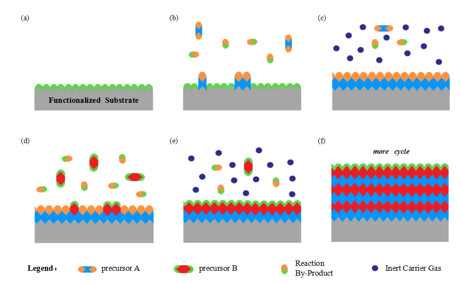
MEMS [22-25] is one of the critical technologies for the development of integrated circuits. It experienced rapid development since the 21st century, and has shown a strong vitality in a number of interdisciplinary areas. Thin film deposition technology, especially ALD technology, is an important process in MEMS surface micro-machining technology. Due to the thin film thickness and complex substrate structure, some models that are more suitable for processing small size are also proposed. Two models suitable for ALD thin film growth and post-deposition pattern prediction are described below.
(1) Cellular Automata Model
Cellular automata (CA) [24, 26-28] is a time-space discrete dynamic system. Each cell has a fixed grid representation and a finite discrete state. According to the same evolution rules, the whole cell is updated when time and local environment change. Due to its simple dynamic system composition, it has the advantage of high precision in three-dimensional space simulation. Cellular automata model is a kind of complex and changeable model without fixed mathematical formula. Among the numerous cellular automata models based on different starting points, the most influential one is the cellular automata classification based on dynamic behavior made by S.Wolfram [27] in the early 1980s, and the cellular automata classification based on dimension is also the simplest and most commonly used classification. For the treatment of thin film growth problem, this model shows its advantages of simplicity and matching with the growth model.
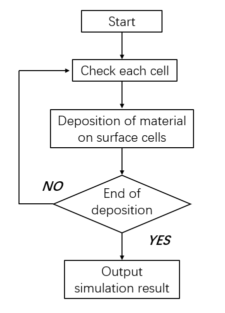
Cellular automata can be divided into the following four methods: Ordinary-CA method, Random-CA method, Continuous-CA method, and Dynamic-CA method. The Ordinary-CA method assumes that there are only two fixed states of atoms on the lattice, and only the principal direction rate is considered in the analysis. The Random-CA method was proposed by Than and Buttgenbach [29] et al., and whether the pre-deposited atom completed the opportunity process depends on a probability parameter P. The model also considers the interaction and connection state between atoms and adjacent atoms, and the probability P can express the deposition influence from different directions. Although this method can deal with the deposition rate in all directions, it is not clear about the boundary and the surface. The Continuous-CA method was proposed by Zhu and Liu [30, 31] et al., where a parameter M is used to represent the continuous state of each atom, and M can be randomly distributed between the two states. In this way, the influencing factors in the Random-CA model can be reduced, the simulation accuracy can be improved, and the surface of simulation results can be no longer fuzzy. Finally, the Dynamic-CA model is proposed by scholars such as Than and Buttgenbach [32], which mainly deals with the behavior of all atoms in the original model and only deals with the atoms related to the deposition surface, greatly improving the computing speed. According to the basic steps of cellular automata method, the computer can carry out sedimentation simulation according to the process in Figure 4.


Figure 4.   Flow chart of cellular automata.
(2) Geometric Modeling
The idea of geometric modeling is to treat the sedimentary surface as a continuous whole [24, 33]. The shape of the sedimentary surface changes according to the geometric rules at certain time steps, and the sedimentary results are related to the geometric rules. Currently, there are about three geometric rules [34-36]: wulff-jaccodine rule proposed by Jaccodine, Slowness rule proposed by Sequin, and e-shapes rule proposed by Hubbard et al. The first rule applies the concept of "plane wave". The current contour surface will move along the normal vector method of contour surface with the growth rate calculated by the process, and will be updated with the number of cycles. The second rule applies the "slow rate" to calculate the trajectory change of the sedimentary surface. The "slow rate" is the reciprocal of the relative rate. In this way, it has a more detailed representation for the edge corner of the spit signal. The third rule introduces the "E vector", which is defined as the vector formed by two adjacent tangent points from the initial point to each unit of time. It combines the characteristics of the above two rules and improves the precision. The use of geometric methods requires that the rate of structural change in the deposition process must be known, and the precision of the model is also determined by the accuracy of the calculation of the rate of change.
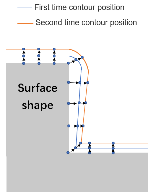
The model can be divided into Line algorithm and Level Set algorithm. Line algorithm is a kind of surface movement algorithm, which discretize the sedimentary surface into equidistant points and calculate the normal vector direction (sedimentary direction) of the point through the relation between the point and the adjacent position. The sedimentary distance is the product of the sedimentary rate and time. After each point changes with the time step, all points are connected with smooth lines in order, which can be expressed as the contour lines of the sedimentary structure [24]. The schematic diagram of line algorithm variation is shown in Figure 5. Level Set algorithm using collective concept, will represent for the curve or surface movement over time than one-dimensional function of zero Level Set function, Level Set, as long as in the process of calculation of the Level Set function derivation on both sides, you can get a partial differential equation, the solution of equation can get evolution after the Level Set function, according to the Level of machine before and after the change, get the movement curve or surface. This model has the advantages of high precision and high efficiency, and can deal with the change of topological form well.


Figure 5.   Schematic diagram of line algorithm.
2.2.3. Multi-scale Modeling of Atomic Layer Deposition
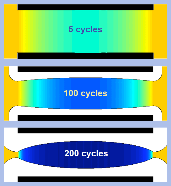
Multi-scale simulation model is a method to study the same problem from different angles. All the methods to solve problems have their incompleteness and limitations. In some "blind areas", other more effective and more accurate methods are used to solve local problems. At last, the whole idea of coordinating the whole situation is used to form a more comprehensive whole to solve problems. This is where the multi-scale model comes in. ALD modeling is suitable for this approach. ALD is a dynamic process with multiple time characteristics, and the time of molecular events within each reaction cycle is relatively fast, while nucleation and stable growth and other processes need a relatively long time to complete. Moreover, its length scale is not uniform, the gas before reaching the surface tends to go through a distance of 100 microns or longer, and the film formed is only the level of angstrom. So you need to split the problem and finally couple it. For example, Raymond A. Adomaitis [37, 38] applied the idea of multi-scale modeling when he studied the deposition of thin films in micron diameter tubular structures with ALD technology and studied the deposition rates in the middle and both sides of the tubes. This model can predict the difference of deposition rates in different positions of the tubes in different cycles, as shown in Figure 6. From the results of simulated deposition, this modeling method has high precision and is suitable for the prediction of post-deposition pattern in ALD process.


Figure 6.   Results of tube atomic layer deposition were simulated in different cycles [38].
3.   Simulation of Atomic Layer Deposition
Atomic layer deposition is a kind of thin film deposition technology. Because of its late appearance, it is the earliest method to simulate the film deposition technology. In the process of simulation, due to the accuracy problem, a more suitable simulation method for atomic layer deposition has been derived. The following is the introduction of the most common, basic simulation method.
3.1.   Quantum Mechanics Method
The model of quantum mechanics is based on the complex principle of quantum mechanics [3, 39-44]. The wave function of condensed matter particle system is calculated, and the parameters such as dynamics and thermodynamics are calculated and solved by the principle of statistics. Finally, the results of the problem are obtained. In the study system, we can describe the problem of electronic structure and some basic physical properties by wave function, including crystal plane, amorphous plane and other impurity defects, electronic structure of atomic configuration, stability of phase structure, energy of point surface defect. The atomic bond strength and thermodynamic function, these parameters can solve many problems, including layer structure and so on. But the complexity of the model is a big problem. Although the model can be solved theoretically, the parameters of film growth are difficult to calculate in practice, so we simplify the method of solving Schrodinger equation and introduce the approximate concept. According to the difference of approximate method, the quantum mechanics method can be generally divided into ab initio method, semi-empirical molecular orbital theory (SMOTS), Density functional theory (DFT), et al. [3] The calculation method of quantum mechanics is often used to predict the electronic structure and reaction mechanism, which has the characteristics of high precision, but the calculation system is small.
3.1.1.   Ab Initio Method
The ab initio method [39, 40, 45-50] does not need any empirical value as a reference, and the calculation is carried out under the three conditions of single electron approximation, non-relativistic approximation and adiabatic approximation. The integral of electrons in all systems is calculated by using the parameters of electron mass, electric quantity and atomic number, and the Schrodinger equation is solved. On this basis, the Hatree-Fock (HF) method is developed to solve the Schrodinger equation, but because the contribution of electrons to energy is neglected, there will be large errors in the analysis of some problems. The method of electron correlation contribution is called post-HF method, which can be subdivided into perturbation theory (MP), coupling cluster theory, (CC) and so on. The calculation cost is higher and less used in the calculation of solid surface chemical reaction. Abhijit [51] and Momoji of Tohoku University in Japan simulated the growth of Aurum atoms on the surface of MgO (100) surface by ab initio calculation and density functional theory, and calculated the adsorption of Aurum on the surface of MgO (100) at different positions. The energy change of diffusion and the morphology of Au diffusion aggregation are incomparable to those of MD and KMC models.
The semi-empirical method is proposed mainly to reduce the computational complexity of ab initio calculation, so it simplifies the wave function, Hamiltonian and integral, and forms three kinds of approximate calculation methods. Although the semi-empirical method greatly reduces the computational complexity of ab initio calculation, its results cannot replace accurate quantum computation.
3.1.2.   Density Universal Function
The density functional theory [45, 46, 52-57] shows that the wave function is regarded as the electron density function or the energy of the system particle is regarded as the function of the electron density so as to simplify the problem and transform the multi-electron problem into a single electron problem. By using the density functional theory, we can change the number of electrons N and the wave function variable 3N into three spatial variables to solve the complex problem, so the process is much simplified. The accuracy can also be guaranteed. Guo-Yong Fang et al., using density functional principle to calculate and analyze the way of SiCl4 and H2O as precursors to form silica under the condition of no catalyst by ALD deposition. The half-step reaction of SiCl4 is the key to determine the reaction rate. Yuniarto, et al. have also studied the ALD deposition of H2O and TMA (Al(CH3)3) by using the density functional principle, and studied the bonding and stability of the two semi-reactive surfaces.
The ab initio calculation and density functional theory are called the first-principles method, correctly describing the states of the atoms and the states of the electrons. However, even the most advanced methods of modern physics and quantum chemistry cannot be used to deal with multi-electron quantum states. Therefore, using the potential function of empirical or semi-empirical parameters as the calculation mode has become the mainstream scheme under limited conditions. It is believed that with the development of quantum technology and computer technology, this method should play an important role in the future accurate simulation of thin film deposition principle.
3.2.   Molecular Mechanics Method (MM)
In principle, the molecular mechanics [58-60] method is based on the classical mechanics theory analysis. The interaction between the molecules in the system is calculated, the parameterization and functional relations are expressed as molecular positions, which include potential function and position parameterization. The potential function is divided into two parts: bonding term and non-bonding term. The bonding term includes the interaction terms such as bond angle, bond stretching, dihedral angle torsion, and non-bonding terms. In non-bonding term, there are van der Waals force term, electrostatic term, etc. The potential function in the system can be calculated according to the mathematical relation of each item, while the position parameterization is changed in form according to the different potential function. Molecular mechanics can be used to calculate the energy and conformation of large systems, but the accuracy is not high, and the structural changes of electrons cannot be predicted.
3.3.   Molecular Dynamics Method (MD)
Molecular dynamics [3, 61-64] simulation is to study the motion state of each example with time from atomic scale using Newtonian mechanics method, such as Newton equation and Hamiltonian equation. The research is related to the time and temperature in the system. The motion state of the particles is determined by analyzing the stress of each particle and solving the position and velocity of each particle at a certain time by classical method. The molecular dynamics method holds that the motion of particles accords with the law of Newtonian motion, and the interaction force between particles is represented by the interaction potential between particles. Once the initial velocity and position of particles and the action potential are determined, the corresponding solutions can be obtained. However, the computational complexity of the molecular dynamics method is very large, and the accuracy of the computer cannot be guaranteed when it is used to simulate a large system, and the hardware of the computer is required to be high. In simulating the film growth, the particles are introduced to the reaction surface one by one, and the initial state (incident angle, velocity, position) of the incident particle is provided as the initial condition. The difference of the main models is derived from the difference of the action potential between different reactants. The time scale of simulating dynamic process is too short (average 10ns, maximum 10μs),) not enough to satisfy the demand of s calculation such as surface growth. In principle, quantum mechanics method, molecular mechanics method and their combination can be used in molecular dynamics simulation. Molecular dynamics can be used to study the effect of initial conditions on the growth of thin films. For example, Yan and et al. [65], they used the MD method to study the dynamics of the low energy Au atom on the surface of Au (111), and calculated the atomic structure of the deposited atom and the surface roughness and coating coverage of the film. The effect of particle energy on the film mass was also studied.
3.4.   Monte Carlo Method (MC)
Monte Carlo [66-70] method is a stochastic simulation method, based on random number and sampling theory to construct a suitable probability model. MC method was proposed in the late 19th century. But the actual use and development was after the popularization of computers. In the 1940s, American scientists applied the design of atomic bomb. The MC model of thin film deposition was proposed by Bruschi [71], and has been improved continuously. Ratsch et al. discussed the influence of experimental conditions (coverage rate and deposition rate etc.) on the growth of surface islands by Monte Carlo method. Considering the possible motion of all particles and giving the corresponding probability, the parameter of the model is the probability or expectation of the event. Then the motion of the particle is assumed by the stochastic principle, and the approximate solution of the problem is obtained by calculating the obtained parameters. This method does not take into account the process quantity of particle motion, but only considers the initial and terminal states (energy, position, etc.) of each motion.
Molecular dynamics simulation and Monte Carlo simulation are two of the most important computer simulation membrane growth methods, because the simulation time of molecular dynamics simulation is long and limited by computer ability. At present, it is not possible to simulate the true film growth process. The Monte Carlo method is suitable for calculating the state of particle system. Although it is difficult to describe the trajectory of particle motion, the Monte Carlo method is suitable for the study of thin film growth because of the small amount of calculation and the reasonable description of the state of the whole system.
In addition to using the above four basic types of calculation and simulation, the atomic layer deposition technique also has a combination of the above basic methods, in order to give full play to the advantages of various methods to deal with the problem of atomic layer deposition.
3.5.   Kinetic Monte Carlo (KMC)
At present, dynamic Monte Carlo [72-76] method is widely used in film growth simulation. For example, Zhou. Wu, et al. [76] have used KMC method to study the process of roughening phase transition on the growth rate and surface morphology of films by temperature. The simulation results show that, when the temperature is lower than the temperature of phase transition, the film is layered and the growth rate is slow. KMC can effectively solve the problem of long treatment time of molecular dynamics. It classifies the movement of ions when the system is in a stable state, and deals with the movement of particles at the bottom of the potential energy well separately from the event types that "evolve" over different potential wells. Therefore, this method can better describe the transition from one state to another, and can achieve a longer time range (more than two seconds), thus saving calculation time in describing the state of particle dynamics as accurately as possible.
3.6.   Lattice Kinetic Monte Carlo Method (LKMC)
Mazaleyrat et al. [75] studied the growth of Al2O3 film on SiO2/Si (100) surface by LKMC [77-80] method. The schematic diagram of simulated deposition principle is shown in Figure 7. The reaction of adsorption and desorption and growth process was simulated by this method. The growth process of ALD was simulated by using this method. LKMC is a comprehensive simulation method. It is a combination of lattice dynamics and Monte Carlo method, and the probability of diffusion is controlled by the interaction potential between adjacent atoms. The change of atomic structure is determined by specific local events and the basic reaction mechanism in special position. The kinetic parameters can be derived from the conversion rate calculated by the activation energy, ALD process parameters and random numbers, and the activation energy data can be derived from the theoretical or experimental data. Because it can simulate the long time and large scale atomic motion process, this method has become a practical method to simulate the growth of thin films. Dynamic lattice Monte Carlo method requires high rationality of modeling. The key of modeling also depends on the determination of the migration process of atoms and the probability of their migration process, which will affect the accuracy of the final results.


Figure 7.   Monte Carlo lattice-based model [75].
3.7 Method of Combining Monte Carlo with Molecular Dynamics
The dynamic Monte Carlo method, which combines molecular dynamics simulation with Monte Carlo simulation, is one of the important methods to study the dynamic simulation of thin film growth. Knizhnik and Bagaturyants, et al. [81] can study the adsorption process of ALD by using this method, which can be divided into two steps. Firstly, the density functional (DFT) is used to calculate the basic reactions. Secondly, the reaction rate is obtained by the traditional kinetic theory, and the film growth is simulated by the kinetic Monte Carlo method according to the adsorption events. Fourthly, the relaxation surface structure of the system is simulated by MM/MD method, and the adsorption process is simulated according to the different coverage of the surface adsorption. The results are in agreement with the results obtained by the DFT method.
And so on, the combination of density functional and Monte Carlo, random deposition and molecular dynamics, and so on, all of which have the advantage of combining to make up for the lack of a single simulation to deal with the ALD problem, so that we can do better. The numerical results are more realistic [82,83].
4   Prospects for Modeling Simulation of Atomic Layer Deposition Technology
With the gradual reduction of the process size, especially when the international advanced manufacturers put forward the requirements of the process size of 7nm and below, the ALD technology has been paid more and more attention, and has been entrusted with important tasks in the design of new structures.
Process equipment companies, such as LAM, APM, Beam, etc., have combed the mainstream applications of ALD [84]. Application 1: "Self-alignment" process, which is a key step of self-aligned double patterning (SADP) technology, the use of ALD technology to fabricate the thin film spacer side wall, thus forming the upper layer of the final figure "mask layer". This can form patterns even smaller than the current lithography resolution. In this technique, film spacers are deposited on predefined features. This interlayer must be highly conformal and very uniform, because it will define the key dimensions of the final pattern. Application 2: 3D NAND requires a high degree of process variability control for 3D storage devices, so ALD technology is suitable to form dielectric films on the sidewall of memory holes. Metal ALD is also used to fill the word line in the alternative gate (gate) scheme. In order to complete the above scheme, it is necessary to better deal with the lateral deposition technology of very narrow size. Application 3: FinFET process, the thin gate side wall of FinFET requires forming a spacer with uniform thickness and no holes. ALD can separate the control gate from the fin structure, which is the best way to deposit the layer.
Modeling of the ALD thin film growth and contour prediction have been realized with improved accuracy with the improvement of computer capability and the addition of novel ideas. For example, the plasma etching model developed by professor Kushner [85] leading the computational plasma science and engineering group has been enlightened, as shown in Figure 8. The accuracy of the model can be greatly improved if the parameters such as particle incidence angle and viscosity coefficient in ALD technology are correctly expressed by means of model particle and grid. In addition, attributing to the development of machine learning, big data and other technologies, the simulation accuracy can be improved in the future through a large number of foundry data and high-precision experimental data, as well as through the continuous training of neural network. The neural network enhances the interaction between data and improves the fitting degree of the model by setting appropriate hidden layers.


Figure 8   Gridding modeling to deal with the problem of atomic layer deposition [85].
It is believed that as more and more attention is paid to the technology of atomic layer deposition, the methods of modeling will become richer and more precise, with the etching process simulation evolution and the emerging of more novel and suitable modeling methods for atomic layer deposition technology, opening windows for better development of the atomic layer deposition technology.
5.   Conclusion
Atomic layer deposition model is derived from thin film deposition modeling in order to develop its own suitable way. The current manners of modeling are getting more diversified, many researchers are trying to combine the various multi-scale modeling ideas that are suitable for ALD in order to build more novel and higher accuracy new models. And ALD process technology itself also evolves along with the shrinking resolution, being more implemented in the integrated circuit manufacturing.
The development of high precision, accuracy and predictability process simulation greatly reduces the unnecessary time lost and cost, greatly increasing the cost performance. In a sum, a high-quality process model is worth our painstaking research.
Acknowledgement
This work was supported by Beijing Natural Fund 4182021 and the National Natural Science Foundation of China 61874002. We are grateful to the School of Information Science and Technology of North China University of Technology (NCUT) for financial support and the Key Laboratory of Microelectronics Devices and Integrated Technology, Institute of Microelectronics, Chinese Academy of Sciences for advising.
[1]R. J. Zhang, et al, Nanscale Integrated Circuits - The Manufacturing Process Second Edition, Beijing: Tsing Hua University Press,2014.7
[2]W. Z. Tang, Preparation principle, Technology and Application of thin Film Materials, Beijing, Metallurgical industry Press, 2003.
[3]A. D. Li, Atomic layer deposition Technology--principle and Application, Beijing, Science Press, 2016.
[4] R. W. Johnson, A. Hultqvist, S. F. Bent, “A brief review of atomic layer deposition: from fundamentals to applications”, J. Materials Today.17(5), 236-246.
[5]J. S. Ponraj, G. Attolini, M. Bosi, “Review on Atomic Layer Deposition and Applications of Oxide Thin Films”, J. Critical Reviews in Solid State & Materials Sciences. 2013, 38(3):203-233.
[6]R. L. Puurunen, “Formation of Metal Oxide Particles in Atomic Layer Deposition During the Chemisorption of Metal Chlorides: A Review”, J. Chemical Vapor Deposition. 2010, 11(2):79-90.
[7]S. D. Athavale, D. J. Economou, “Realization of atomic layer etching of silicon”, J. Journal of vacuum science & technology. B, Microelectronics and nanometer structures: processing, measurement, and phenomena: an official journal of the American Vacuum Society. 1996, 14(6):3702-3705.
[8]K. J. Kanarik, T. Lill, E. A. Hudson, et al. “Overview of atomic layer etching in the semiconductor industry”, J. Journal of Vacuum Science & Technology A Vacuum Surfaces & Films. 2015, 33(2):020802.
[9]Athavale, D. Satish, “Molecular dynamics simulation of atomic layer etching of silicon”, J. Journal of Vacuum Science & Technology A: Vacuum, Surfaces, and Films. 1995, 13(3):966.
[10]Y. J. Jin and L. H. Fujiwara, Wang and H. T. Zheng (Translate), thin film. Beijing. Publishing House of Electronics Industry.1988.
[11]X. Li and G. M. Xiong, “Calculation of order parameters in Surface adsorption State Simulation by Lattice Gas Model”, J. Journal of Atomic and Molecular Physics. 2001(03):325-328.
[12]G. M. Xiong and Xia. Li. “Monte Carlo investigation of adsorption stage of O on Ru(0001):a study of a lattice mode”, J. Commum Theor Phys.(Beijing China)2001,35,114~117
[13]T. A. Witten, Jr. And L. M. Sander, “Diffusion-Limited Aggregation, a Kinetic Critical Phenomenon”, J. Physical Review Letters, 47(19), 1400–1403.
[14]Fang. Fang and Jinming Liu, “Diffusion limited aggregation model”, J. Chinese Journal of Nature,2004(04):200-205.
[15]E. Somfai, R. C. Ball, N. E. Bowler., et al, “Correction to scaling analysis of diffusion - limited aggregation”, J. Physica A Statistical Mechanics & Its Applications, 2003, 325(1):19-25.
[16]T. Michely, M. Hohage, M. Bott, et a, “Inversion of growth speed anisotropy in two dimensions”, J. Physical Review Letters, 1993, 70(25):3943-3946.
[17] B. G. Liu, J. Wu, E. G. Wang and Z. Y. Zhang, “Two-Dimensional Pattern Formation in Surfactant-Mediated Epitaxial Growth”, J. Physical Review Letters, 83(6), 1195–1198.(1999)
[18]E. G. Wang, Progress in Physics 23 1(in Chinese),2003
[19]M. Copel, M. C. Reuter, E. Kaxiras and R. M. Tromp, “Surfactants in epitaxial growth”, J. Physical Review Letters, 63(6), 632–635.(1989)
[20]I. S. Hwang, et al. “Mechanisms and energetics of site hopping and chemical reactions of O2 molecules at Si(111)-7 × 7 surfaces”, J. Surface Science, 399(2-3), 173–189.(1998)
[21]J. Tang, X. Q. Yang, K. Chou, “Study on the Dynamic Behavior of the Reaction-limited Aggregate Model”, J. Acta Physica Sinica,2005(07):3307-3311.
[22]M. G. Hankins, P. J. Snick, D. M. Tanner, et al, “Vapor deposition of amino-functionalized self-assembled monolayers on MEMS”, C. Reliability, Testing, & Characterization of Mems/moems II. 2003.
[23]N. Hoivik, J. W. Elam, S. M. George, et al, “Atomic layer deposition (ALD) technology for reliable RF MEMS”, C. International Microwave Symposium Digest. IEEE, 2002.
[24]Haiquan. Zhou, “Simulation of PECVD Deposition Based on Level Set”, D. Jiangsu: Southeast University, 2014
[25]L. Jiang, R. Cheung, “A review of silicon carbide development in MEMS applications”, J. International Journal of Computational Materials Science and Surface Engineering, 2009, 2(3/4):227.
[26]S. Misra, A. K. Das, D. R. Chowdhury, et al, “Cellular Automata—Theory and Applications”, J. IETE Journal of Research, 1990, 36(3-4):9.
[27]S. Wolfram, “Cellular automata as models of complexity”, J. Nature, 311(5985), 419–424. doi:10.1038/311419a0
[28]A. Crooks, Cellular Automata M. The International Encyclopedia of Geography. John Wiley & Sons, Ltd, 2017.
[29]O. THAN, S. BUTTGENBACH, “Simulation of anisotropic chemical etching of crystalline silicon using a cellular automata model”, J. Sensors and Actuators A: Physical, 1994, 45(1):85-89.
[30]Z. ZHU, C. LIU, “Micromachining process simulation using a continuous cellular automata method”, J . Journal of Micro-electro-mechanical Systems, 2000, 9(2):252-261.
[31]Z. ZHU, C. LIU, “Simulation of anisotropic crystalline etching using a continuous cellular automata algorithm”, J. CMES- Computer Modeling in Engineering & Sciences, 2000, 1(1):11-19.
[32]S. Bttgenbach, O. THAN, “SUZANA: A 3D CAD Tool for Anisotropically Etched Silicon Microstructures”, J. 1996.
[33]Udeshi, Tushar, “ACM Press the 2005 ACM symposium - Cambridge, Massachusetts (2005.06.13-2005.06.15)] Proceedings of the 2005 ACM symposium on Solid and physical modeling, - SPM \"05 - Accurate and robust geometric modeling for simulation of IC and MEMS fabrication processes”, J. 2005:257-266.
[34]R. J. Jaccodine, “Use of modified free energy theorems to predict equilibrium growing and etching shapes”, J. Journal of Applied Physics, 1962, 33(8):2643-2647
[35]C. H. Sequin, “Computer simulation of anisotropic crystal etching”, J . Sensors and Actuators A: Physical, 1992, 34(3):225-241.
[36]T. J. Hubbard, E. K. Antonsson, “Emergent faces in crystal etching”, J . Micro-electro- mechanica 'systems, 1994, 3(1):19-28.
[37]R. A. Adomaitis, “Development of a multi-scale model for an atomic layer deposition process”, J . Journal of Crystal Growth, 2010, 312(8):1449-1452..
[38]V. Dwivedi, R. A. Adomaitis, “Multi-scale modeling of atomic layer deposition processes”, C. American Control Conference. IEEE, 2009.
[39]I. N. Levine, quantum chemistry, Beijing: World Book Inc,2011
[40]E. G. Lewars, Computational Chemistry: an introduction to the Theory of Molecular and Quantum Mechanics and its applications, Beijing: Science Press,2012
[41]MengHai. Lin, Brief course on Quantum Chemistry, Beijing: Chemical Industry Press,2005
[42]JingJiang Liu, Application of basic quantum chemistry, Beijing: Higher Education Press, 2004.
[43]Chengda Zhao, The theoretical basis of solid Quantum Chemistry and material Chemistry Version 2,Beijing:Higher Education Press, 2003.
[44]P. Song, JiangSheng. Lu, Q. Hu, et al, “Application and Development of computer Simulation on deposition Mechanism of thin Films”, J. 2003(S1):154-157.
[45]P. Hohenberg, W. Kohn, “Inhomogeneous electron gas”, J. Phys.Rev,1964,136 (3B): B864-B870.
[46]W. Kohn, L. J. Sham, “Self -Consistent equations including exchange and correlation effects”, J. Phys Rev, 1965,140( 4A):A1133-A1138.
[47]T. Tomohito, M. Katsuyuki, I. Yuichi, “First - principles study on structures and energetics of intrinsic vacancies in SrTiO3”, J. Phys Rev, B: Condens Matter,2003,68 (20) : 205213-1- 205213-8.
[48]M. Arques, L. K. Teles, V. Anjos, et al, “Full-relativistic calculations of the SrTiO3 carrier effective mass and complex dielectric function”, J. Appl Phys.Lett,2003,82(18):3074-3076.
[49]J. HAY.P, W. R. WADT, “Ab initio efective core potential for moleculat calculation”, J. J.Chem Phys, 1985,82:270-284.
[50]J. HAY.P, W. R. WADT. “Ab initio effective core potentials for molecular calculations for K to Au including the outermost core orbitals"”, J. J Chem Phys, 1985,82:299-310.
[51]A. Chatterjee, M. Kubo, K. Teraishi, et al, “Application of integrated computer simulation approach to solid surfaces and interfaces”, J. Catalysis Surveys from Asia, 1998, 2(2):133-153.
[52]G. Fang, et al, “Stepwise mechanism and H2O-assisted hydrolysis in atomic layer deposition of SiO2 without a catalyst”, J. Nanoscale Research Letters, 10(1).
[53]Y. Widjaja and C. B. Musgrave, “Quantum chemical study of the mechanism of aluminum oxide atomic layer deposition.”, J. Applied Physics Letters,80(18), 3304-3306.
[54] Y. Widjaja and C. B. Musgrave, “Atomic layer deposition of hafnium oxide: A detailed reaction mechanism from first principles”, J. The Journal of Chemical Physics,117(5), 1931-1934.
[55]J. Ren, F. W. Liu, Y. T. Zhang, D. W. Zhang, “Initial reaction of HfO2 atomic layer deposition on silicon surfaces with different oxygen levels: A density functional theory study”, J. Thin Solid Films, 515(11), 4702-4708.
[56]J. Ren, B. Sun, D. W. Zhang, “Density functional study of initial HfCl4 adsorption and decomposition reactions on silicon surfaces with SiON interfacial layer”, J. Applied Surface Science, 253(23), 9148-9153.
[57] J. Ren, Y. T. Zhang, D. W. Zhang, “Density functional theory study of initial stage of HfO2 atomic layer deposition on hydroxylated SiO2 surface”, J. Journal of Molecular Structure: THEOCHEM, 803(1-3), 23-28.
[58]M. B. Chen, Computational Chemistry: from theoretical Chemistry to Molecular Simulation, Beijing: Science Press,2009
[59]Leach A.R. The principle and Application of Molecular Simulation Version2 ,Beijing, World Book Inc ,2003
[60]D. Rob, Computational material science. Beijing: Chemical Industry Press,2002
[61] Kato. Seizo, Hangxiang. Hu. “Moleeular dyanmics simulation of the thin film fabrication process”, J. Surf Sci,1996,357:89
[62]Dong Liang, Richard W Simth, David J Srolovitz, “A two-dimensional molecular dynamics simulation of thin film growth by oblique deposition”, J. Appl Phys,1996,80(10):5682
[63]L. F. Qi, et al. “Effeet of surface reactivity on the nuele-ation of hydroearbon thin films through moleeular-cluster beam deposition”, J. Surf Sci,1999,426:83
[64]Z. H. Chen, C. Y. Yu, P. F. Lu, Y. M. Liu, Y. G. Wang, “Molecular Dynamics Simulation of GaN thin Film growth”, J. Journal of Functional Materials, 2008,39(12):2045-2048.
[65]C. Yan, L. L. Huang, X. D. He, “Molecular dynamics simulation of the influence of incident energy on the growth of Au/Au _ (111) thin films”, J. Acta Physica Sinica, 2014, 63(12 ):283-291.
[66]S. Ozawa, Y. Sasajima, D. W. Heermann, “Monte Carlo simulation so thin growth. ”, J. Thin Solid Films,1996,272:172
[67]Z. J. Xu. Monte Carlo method, ShangHai, Shanghai Scientific & Technical Publishers,1985
[68]H. Huang, and G. Gilmer, “Atomistic simulation of texture competition during thin film deposition”, J. Journal of Computer-Aided Materials Design, 7(3), 203–216.
[69] H. Huang, and G. Gilmer, “Multi-lattice Monte Carlo model of thin films”, J. Journal of Computer-Aided Materials Design, 6(2/3),117-127.
[70]D. Frenkel, B. Smit. Introduction to Molecular Simulation Version2 ,Beijing, World Book Inc ,2010
[71]P. Bruschi, P. Cagnoni, A. Nannini, “Temperature-dependent Monte Carlo simulations of thin metal film growth and percolation”, J. Physical Review B, 55(12), 7955-7963.
[72] T. A. Witten, L. M. Sander, “Diffusion-limited aggregation: A kinetic critical phenomenon? ”, J. Contemporary Physics, 41(4), 203-218.
[73]J. Salik, “Monte Carlo study of reversible growth of clusters on a surface”, J. Physical Review B, 32(3), 1824-1826.
[74]Z. Zhang, X. Chen, M. G. Lagally, “Bonding-Geometry Dependence of Fractal Growth on Metal Surfaces”, J. Physical Review Letters, 73(13), 1829-1832.
[75]G. Mazaleyrat, A. Estève, L. Jeloaica, et al. “A methodology for the kinetic Monte Carlo simulation of alumina atomic layer deposition onto silicon”, J. Computational Materials Science, 2005, 33(1-3):0-82.
[76]X. F. Zhou, C. Wu, C. Y. Tang, C. G. Kong, B. B. Qiu, Y. Yang, G. W. Lu, “Dynamic Monte Carlo (KMC) simulation of thin film growth”, J. Journal of Synthetic Crystals, 2012,41(03):792-797.
[77]Z. R. Wu, X. B. Cheng, Z. S. Wang, “Simulation of Cu thin Film growth by dynamic Lattice Monte Carlo method”, J. ACTA PHOTONICA SINICA, 2010,39(01):62-66.
[78]Y. Guo, G. Wang, C. Zhao, J. Luo, “Simulation and characterization of stress in FinFETs using novel LKMC and nanobeam diffraction methods”, J. Journal of Semiconductors, 36(8),086001.
[79]Z. Wang, Y. Li, J. B. Adams, “Kinetic lattice Monte Carlo simulation of facet growth rate”, J. Surface Science, 2000, 450(1):51-63.
[80] J. B. Adams, Z. Wang, Y. Li, “Modeling Cu thin film growth”, J. Thin Solid Films, 2000, 365(2):201-210.
[81]A. A. Knizhnik, A. A. Bagaturyants, I. V. Belov, et al. “An integrated kinetic Monte Carlo molecular dynamics approach for film growth modeling and simulation: ZrO2 deposition on Si(100) surface”, J. Computational Materials Science, 2002, 24(1-2):128-132.
[82]Z. Hu, J. Shi, C. H. Turner, “Molecular dynamics simulation of the Al2O3 film structure during atomic layer deposition”, J. Molecular Simulation, 2009, 35(4):10.
[83]A. A. Knizhnik, A. A. Bagaturyants, I. V. Belov, et al, “An integrated kinetic Monte Carlo molecular dynamics approach for film growth modeling and simulation: ZrO2 deposition on Si(100) surface”, J. Computational Materials Science, 2002, 24(1-2):128-132.
[84]https://blog.lamresearch.com/tech-brief-a-look-at-atomic-layer-deposition-ald/
[85]T. J. Sommerer, M. J. Kushner, “Monte Carlo‐fluid model of chlorine atom production in Cl2, HCl, and CCl4 radio‐frequency discharges for plasma etching”, J. Journal of Vacuum Science Technology B Microelectronics & Nanometer Structures, 1992, 10(5):2179-2187.
Article and author information
Lei Qu
Rui Chen
Xiaoting Li
Jing Zhang
Yanrong Wang
Shuhua Wei
Jiang Yan
Yayi Wei
Publication records
Published: June 26, 2019 (Versions2
References
Journal of Microelectronic Manufacturing