Research Article Current Issue Versions 2 Vol 3 (4) : 20030406 2020
Download
Material Modeling in Semiconductor Process Applications
: 2020 - 10 - 01
: 2020 - 11 - 02
: 2020 - 12 - 30
2465 49 0
Abstract & Keywords
Abstract: During the past decade, significant progress has been achieved in the application of material modeling to aid technology development in semiconductor manufacturing companies such as Intel. In this paper, we review examples of applications involving a complex set of material modeling tools and methodologies and share our perspective of the future of the area. Examples are given illustrating the landscape of useful physical models and approaches along with commentary addressing tool relevance and simulation efficiency issues. While the scope of this paper precludes providing in-depth details, references to more focused publications are shared. Finally, we outline how to approach constructing a general infrastructure for supporting TCAD material modeling applications.
Keywords: TCAD; atomistic modeling; density functional theory; molecular dynamics; kinetic Monte Carlo
1.   Introduction
In the past thirty years, semiconductor modeling in industrial TCAD (Technology Computer Aided Design) has undergone incredible change. Over this period, device engineering has evolved dramatically with the introduction of the FinFET, novel materials, and strain. In addition, the concentration of fabrication facilities within just a few large companies has resulted in TCAD departments becoming more active in conducting in-house research versus relying on external sources. However, the single biggest change for TCAD is undoubtedly the scale of the problems it now tackles. In the 1990’s, TCAD was concerned almost solely with simulating device performance, which meant figuring out how to control short channel effects (SCE) as the gate length shrunk by simulating various S/D and well engineering options. The modeling domain for this problem was confined to 100’s of nanometers. Today, the scale of problems extends over 8 orders of magnitude. Stress engineering has moved the simulation domain beyond the device itself to including neighboring structures which also impacts the mechanical stress in the channel. Parasitic effects like latch-up and reliability phenomenon such as ion strikes require even larger scale simulations. At the upper end, calculating attributes such as die temperature, which requires simulating the heat generated from every transistor and interconnect, has extended the domain to millimeters. On the small end of the scale, features of the device such as fin width are now down to a countable number of atomic layers. As a result, TCAD must rigorously calculate quantum effects such as confinement and tunneling and also fundamental material properties, which depend not only on the novel materials employed but also on the specific number of layers. At the atomic scale, the impact of defects, which can cause changes in intrinsic strain, leakage, and resistance in semiconductors and metals, are now routinely estimated with modeling. TCAD is even tasked with simulating the properties of individual molecules such as adhesion and selectivity to help down select the reagents used in process steps such as Atomic Layer Deposition (ALD). As technology continues to scale, device and process modeling is evolving into an extended materials problem.


Figure 1.   Time and length scales and schematics of methodologies of material modeling. Arrows show the information flow between methodologies.
As a result, material modeling (MM) has become an essential part of TCAD domain along side more tradition disciplines. While scaling provides the motivation for this evolution, what has made MM possible is the tremendous progress in the development of computational methods for many-body interacting systems[1] and the incredible advances in computing power [2]. The role of MM in TCAD is twofold. On one hand, MM is used to analyze the behavior of novel structures and materials on the atomic to nanometer size scale. On the other hand, researchers also resort to MM when the validity of parameters used in macroscopic simulations, which are based on continuous models, become questionable, such as when materials are employed at such a minute scale that their bulk properties no longer apply. A good example of this is understanding the heat transfer across the interface of two dissimilar materials[3]. In the case of nonmetals, where phonons are responsible for the energy transfer, the continuous heat transfer (Fourier) model fails at a length scale comparable to the average phonon mean free path, giving rise to the interface thermal resistance. From the macroscopic point of view, the temperature looks discontinuous on the interface, but by employing an MM approach such as molecular dynamics (MD) simulation[4], the energy flux can be calculated and used to extract the coefficient of interface thermal resistance, which can then be inserted into the continuous heat transfer model.
Overall, the limitation of continuum models is that most assume certain constitutive relations to describe material properties, e.g. stress versus strain dependence for mechanical properties or diffusivity dependence on the temperature. These assumptions are clearly violated on the nanoscale. In contrast, when one is applying an MM approach, the only assumption is how atoms or molecules interact directly with each other. This interaction can be treated as either classically or quantum mechanically. In the classical case, the system energy is represented as a sum of contributions from a pair or many-body potentials over all atoms in the system. In the quantum treatment, the energy of electrons interacting with both ions and other electrons and the ions among themselves are calculated using the quantum theory of many-body systems. There are numerous methods for these calculations; among them, the Density Functional Theory (DFT)[5] is the most frequently used approach. It worth noting that in a TCAD context, the material subject to modeling is, as a rule, assumed to be in the solid state.
2.   Applications of Material Modeling
Table 1 shows a brief list of MM applications that are relevant to semiconductor technology development and are currently in use in industrial TCAD. This list is not comprehensive and focuses primarily on applications in TCAD’s traditional scope. The objective of this section is to elaborate on the content of this list.
 Table 1. Material modeling applications.
 
Application domainProperties of interest
Pure and compound bulk materialsEquilibrium structure, stability, equation of state, mechanical, thermophysical, heat and electric transport, electronic structure, vibration spectra
Point and extended defectsStructure, formation energy, electronic structure, optic absorption, diffusivity, fracture, plasticity
2D heterostructures, interfaces, thin films, free surfacesStructure and defects, stability, transport, electronic structure, surface reconstruction and chemistry
Atomistic processes, etching, deposition, epitaxial growthSelectivity, byproducts yield, effect of process conditions, microstructure formation and evolution, material damage and recrystallization
3D nanostructuresGrain structure, contacts, conductance, strain, effect of size
Historically, the aim of statistical physics and condensed matter theory was the calculation of bulk properties of pure and compound homogeneous materials, where it achieved remarkable progress. To a greater degree, this progress was attributed to the fact that, for an ideal crystal, lattice electron wave functions can be relatively easy constructed as well as quantum mechanically methods to self-consistently account for non-weak many-body interactionsin solids[6]. In today’s DFT based computational tools, the analogous problem is choosing an appropriate electron basis function (either plane waves or atomic orbitals depending on the type of material – metal or non-metal) and a suitable form of the exchange-correlation functional[5]. These calculations don’t require significant computational resources since just a single crystal cell can be used to deliver a wide variety of material properties including: the geometry of the crystal cell minimizing the total system energy and thus material density, its formation (cohesive) energy, elastic moduli as derivatives of the total energy versus the cell volume and strain, etc. A more extended theory allows the definition and quantification of the effects of elementary quantum excitations in solids – quasiparticles such as electrons, holes, and phonons[7]. Most available DFT packages[8] can calculate properties of these particles such as band structure and the phonon spectrum. With this information, one can assess transport and thermal material properties at finite temperatures such as heat capacity, thermal and electrical conductivity. This is for an ideal crystalline material, which allows the reduction of the computational domain to a single lattice cell and limits the number of atoms under consideration to just a few, explaining why the computational burden for this sort of calculation is modest. It should be noted that the complex quantum computations above can be bypassed if a sufficiently accurate interatomic interaction potential is known a priori which allows calculation of the total system energy. More details about this approach are described in Section 3.
The situation changes in real materials where nonuniformities, such as defects, are present.[9] Defects profoundly affect material properties on the nanoscale. In this situation, one faces a dilemma on how to construct the simulation domain, i.e. place the defect into a simulation “box” with periodic boundary conditions or insert it into a finite sample of the crystal lattice. In the first case, an artificial periodic lattice of defects will arise, which requires devising a physical way to account for their interaction energy, especially for charged defects. In the second case, one needs to extend the size of the box to ensure the results aren’t sensitive to the boundary conditions. In both cases, a system with defects becomes much more computationally challenging to simulate compared to ideal crystals. Additional complications arise when we account for defect migration in realistic systems, where the positions of the lattice atoms are modulated by nearby vacancies, thus varying the potential barriers from site to site. This situation not only requires considering numerous intermediate states between the initial and final locations of the atom, but also an effective optimization technique to find the minimal energy path (MEP) associated with the transition[10]. Techniques such as the nudged elastic band (NEB) or the zero temperature string (ZTS) are available in some DFT[11] and molecular dynamics (MD)[12] packages. An extreme but very important case of materials with defects is related to highly disordered systems – amorphous states, random alloys, non-stochiometric compounds, etc. These materials have been a topic of great interest in microelectronics, e.g. non-stochiometric metal oxides are being evaluated in ReRAM device studies[13]. Many of these materials are comprised of random local arrangements of atoms and are not thermodynamically stable, requiring the use of stochastic methods to calculate their properties and to generate representative samples for simulation [14].
An area of great recent activity in MM involves low dimension systems such as free solid surfaces, thin films, material interfaces[15,16,17], motivated by continued scaling which has confounded bulk and interface effects within devices and also by the wafer level chemistry which occurs within the first few atomic layers of the surface. Addressing the problems of interest in these systems goes beyond determining static properties of materials and structures; it requires modeling dynamic processes such as the effect of deposition rate on the crystal structure of the film and how active molecules in a plasma interact with the silicon surface, etc. It also adds complexity because less can safely be assumed about the system without unphysically biasing the solution. Although it has limitations, the MD method has been indispensable tool for modeling these low dimensional systems as discussed in the following section. Many DFT packages are capable of simulating systems with the ab initio MD[18] algorithm; however, computational resources and the turn-around-time to complete simulations are far from what technology engineers would like to see for evaluation of multiple options or optimization of processes.
The final MM application area we will cover is simulation of nanostructures such as nanowires, nanosheets[19,20]. With the reduction of the system size, the “golden age” of being able to use MM only for the extraction of material parameters while doing the brunt of the calculation with more efficient “continuous models” which use those parameters, is waning. The MM methodology is now often applied to the entire structure and used to directly calculate macroscopic characteristics such as the current-voltage relations with methods like the non-equilibrium Green’s function (NEGF)[21] or the time dependent DFT[22]. This along with advancements to the fundamental theory which has been used for computation of ideal crystalline material properties for decades, profound progress in the development of numerical methods, software implementation, and high performance computing has advanced MM capabilities to the point of making them practical for semiconductor technology development.
3.   Metals Intermixing
Metals are a key material in manufacturing high density interconnects (IC) for very large scale integration (VLSI) circuits. The design of an effective IC system is guided by many factors, among them continued scale reduction, low line resistance, minimal crosstalk, and acceptable long term reliability, e.g. mitigation of electromigration effects [23]. This multidimensional optimization results in IC systems composed of different metals and necessarily assumes contacts between them. It is a well-known effect that certain metals used in combination are susceptible to mixing caused by the process of interdiffusion[24]. This process can be intensified with pressure, applied electrical potential, and elevated temperature[25,26]. For some applications, metal interdiffusion is a desirable effect, harnessed to form a mechanically strong joint; however, for the majority of IC processing, this is not the goal. Metals with heterogenous crystal structures and foreign atoms usually increase the resistance of the contacts [17]. The mixing issue is a problem because many IC recipes require depositing thin barrier metal liner first, before the main IC metal. This liner serves as a diffusion barrier for the main contact metal, specifically to prevent its penetration into the inter-layer dielectric (ILD).[27] Mixing between the contact and liner metal would not only destroy this barrier but also increase electrons scattering from the interface, increasing overall line resistance. This is a complex system to simulate which we will discuss in subsequent sections.
3.1.   Thermodynamic Considerations
Metals will intermix only if it’s energetically preferable. For many two-metal combinations, one can usually find in metallurgical textbooks or online databases, an equilibrium phase diagram[28,29] and a graph of mixing enthalpy dependence versus alloy composition to see if the metals in question form an equilibrium binary alloy and thus mix. Complications begin when the metals or their composition is not a popular entity and thus the data is absent. In this case, the mixing enthalpy needs to be calculated. There are two widely used ways to compute the equilibrium state energy of a solid. The first relies on the classical molecular dynamics (MD) method[30]. This method requires a trustworthy interatomic potential, also called a force field (FF), which may not be available for the materials of interest. Fortunately there is a universal FF that works well for metals known as EAM[31], but it requires parameters for the specific metals. If these aren’t available, a standard method for computing these consists of generating a representative set of targets for fitting, a validation suite for testing the result, and a method for optimizing, available from several optimization libraries[32]. The process of optimization itself can involve many stages, such as adding more and more targets to narrow down the set of potential parameters. The targets usually include both experimental data such as material density, elastic moduli, formation energy, etc, and data generated with a more rigorous computational method e.g. DFT[5]. Since most of the targets have error bars, the optimization can be quite complex. It’s worth noting that because of its rigor, the DFT method could be used to calculate the material properties of interest directly; however, DFT doesn’t always reproduce experimental results, even for bulk quantities such as bandgap. Because of this, using an efficient FF with its additional fitting parameters often allows more faithful matches to experiment. This fitting process is also applicable to other systems, for instances those with more than two metals or containing defects. Once the mixing enthalpy has been calculated, its sign suggests whether it’s thermodynamically preferable for two metals to mix at equilibrium conditions or exist as separate phases. The result, however, doesn’t indicate how long it would take for the materials to mix; that is where the process kinetics simulation comes into play which is the subject of the next section.
3.2.   Kinetic Considerations
To evaluate the time scale of intermixing and its dependence on the initial state of the structure and process conditions, a kinetic model of the system must be developed. For this endeavor, one might be tempted to employ the same MD approach used to calculate the energy of the system as described above. However, directly integrating equations of motion for all atoms in the solid results in issue with the time scales involved. To resolve thermal vibrations of atoms, i.e. phonons, one needs to limit the time step at least by the inverse of the typical phonon frequency, which in practical simulations of solids appears to be ~10-2 ps. However, diffusion of atoms in solids is inherently a slow process; observable concentration changes occurs at a time scale closer to ~10-3 sec [33]. The result is that the MD approach becomes computationally prohibitive for modeling solid state diffusion. Another significant caveat is that the FF used in MD simulation would need to be specially fit to reproduce states with atoms far from their equilibrium positions in the crystal lattice, to capture hopping between sites, and not just for the equilibrium properties discussed in Section 3.1. To overcome these issues, the kinetic Monte Carlo (KMC) method[34] can be applied. In this method, a restricted set of physical events is selected and the appropriate rates are calculated for each of event. A Monte Carlo method is then used to sample events and advance the state of the system. In the simplest version of this method, lattice KMC (KLMC), atoms can take only fixed positions in the ideal crystal lattice. An open source implementation of the KLMC is available called SPPARKS[35]. To simulate interdiffusion, we use a customized version implemented with a model known as the binary alloy with vacancies (ABV)[36] model. In this model, a lattice site can be occupied by either atom of type A or B or remain vacant. A simple Hamiltonian, limited to only nearest neighbor interactions, is expressed as a sum of bond energies and depends on six parameters whose values can be fitted to pure metal formation energies, the energy of insertion a foreign atom or the mixing enthalpy, and the energy of vacancy formation. While rather simple, the model allows important observations about the behavior of the system. First, the possibility of mixing is directly related to the sign of AB bond energy; positive values prevent mixing. For interdiffusion to proceed, a sufficient concentration of vacancies must be assigned to the initial state, but not so that high that vacancies can coalesce and form voids. Fortunately, the final configuration is insensitive to the initial distribution of vacancies due to their high mobility. Typically the average time step is ~10-12-10-13 sec unless the Metropolis MC algorithm[37] is selected, which effectively minimizes the system energy to reach the final configuration. These simulations don’t require significant computational resources, e.g. a system of ~105 atoms simulating with SPPARKS using 4-8 parallel processes takes <20 min to reach the final state after ~108 diffusion events. Some examples of simulation results are shown in Figure 2 for the case of good mixing of Al and Cu. The pictures have been created using OVITO[38] which is a very useful tool for visualizing atomistic simulation results.
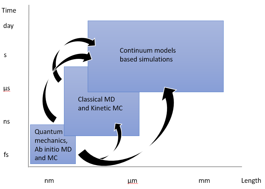
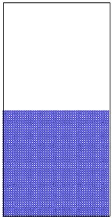
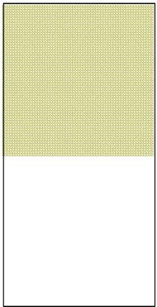
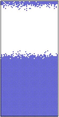
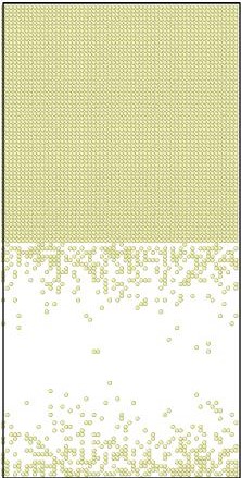
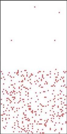
 
Figure 2.   Initial (top 3 panels) and final (bottom 3 panels) states for Al (blue), Cu (yellow), and vacancies (red) shown left to right respectively. The final states after using KLMC to simulate 108 diffusion events in ~10μs . Periodic boundary conditions are set in all directions to avoid a free surface. An Cu-Al alloy forms along the interface separating initially pure metals while vacancies, which are distributed uniformly at the beginning of simulation, move into the Al region.
The KLMC method offers some insights into the kinetics of the intermixing although the experimental data[24] suggest that it’s a much more complex process. Specifically, the main assumption in the KLMC model that atoms hop between sites in a rigid lattice is questionable. During processing, the lattice distorts and many intermediate phases of alloy are formed along the interface. Also, for technology applications, it’s sometimes of interest to evaluate metals with different lattice types and imperfect crystal barrier layers, i.e. those with a grain structure. To address these problems, the off-lattice KMC model[39] has gained attention. KMC differs from KLMC in that it tracks the evolution of the system energy landscape, allowing atoms to occupy any local energy and hop through saddle-points between them. The locations of the minima and corresponding transition barriers are calculated on-the-fly using a suitable FF after every diffusion event, which makes the method extremely numerically expensive; identical systems take ~103 times longer to simulate with KMC versus KLMC, limiting its use [40]. The art of creating a practical KMC code is all about handling fast diffusion events[41], making full use of parallel computing[42], and avoiding barriers recalculation wherever possible
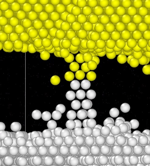
[43]. As we have found at Intel, the pay-off of KMC is the quantitative agreement with experiment for interdiffusion coefficients and activation energies and the qualitative impact of lattice type, orientation, and grain boundaries. An example of its application is illustrated in Figure 3, which shows a FCC Cu - FCC Al bilayer separated with 25A of BCC Ta following 5 μs anneal at 700K. A bridge of Cu and Al atoms formed along the grain boundary through the barrier layer can be clearly seen after 4 days of modeling using 16 parallel processes. It’s also evident that the perfect crystalline Ta is all but immiscible with both Cu and Al.


Figure 3.   The bridge of Al (white) and Cu (yellow) atoms growing through Ta (hidden) separation layer along the grain boundary.
It should be noted that the MD method, despite its limitations, is being used for these type of simulations [25,26]. While certain assumptions help make these simulations more applicable, a pure metal EAM FF is not sufficient for interdiffusion simulations. The FF must include cross-type interactions of metal atoms[44] or hybridization as available in MD codes such as LAMMPS[12].
4. Metal Deposition for Electronic Property Calculations
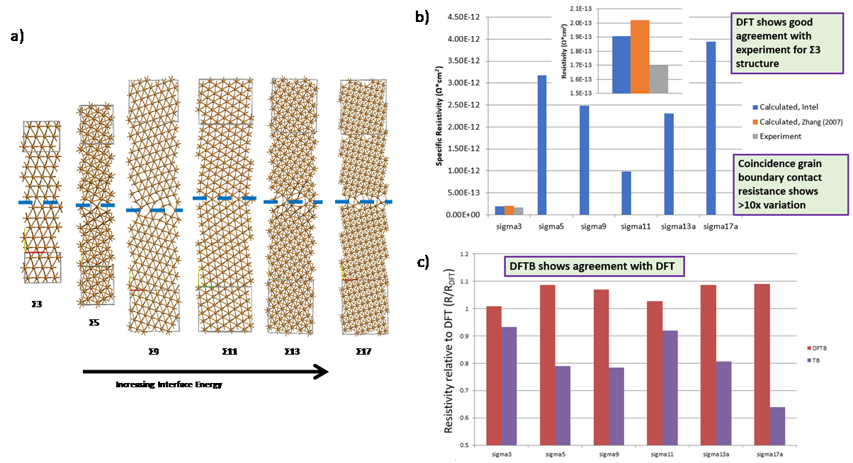
The line resistance of Cu interconnects is shown to be determined by the dimensions, texture and interfaces of the metal. In this section we describe the methodology used to accurately represent the Cu microstructure in planar and trench geometries for use as metal interconnects in integrated circuits. Atomistic representations may be created analytically for bulk and planar polycrystalline configurations, followed by an energy minimization step using LAMMPS[12]. Figure 4(a) shows the generated polycrystalline representation of different grain orientations and boundary interfaces for the most stable Cu textures, generated by rotating perfect crystals to give a single grain boundary. Resistivity of the structures was calculated from using the Nonequilibrium Greens Functions framework [45]. Figure 4(b) shows the resistivities calculated using DFT simulations and compared to experimental and external reports[46]. The computationally faster method of Density Functional Tight Binding (DFTB) [47] was shown to give similar resistances as DFT simulations (see Figure 4(c)) and can be used for larger multi-grain structures with mixed grain boundary types. It is more accurate than using Tight Binding (TB) with parameters from Papaconstantopoulos [48].


Figure 4.   
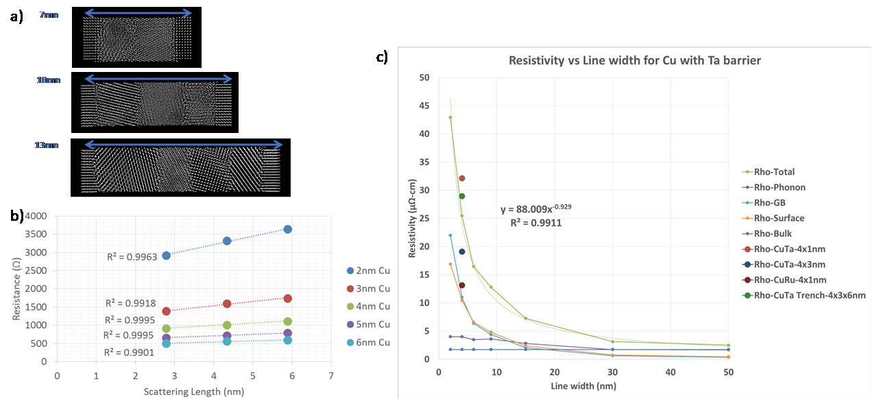
a) Analytically generated polycrystalline FCC Cu grain structures for different sigma grain boundaries. b) calculated resistivity for specific grain boundaries. c) comparison of TB and DFTB resistivity for different grain boundaries relative to DFT.
Using larger analytic polycrystalline structure, over 150 configurations with roughly uniform grain sizes averaging from 2-6nm in size for 3 different lengths ranging from 7-13nm long (see Figure 5(a)) were used to calculate transmission. From these length dependent resistance plots shown in Figure 5(b), the resistivity as a function of grain size was extracted, showing smaller grains lead to higher resistivity due to increased scattering at grain boundaries. Assuming grain sizes proportional to line widths, the resistivity of interconnects including the components extracted for GB & surface scattering can be plotted as shown in Figure 5(c) showing the expected rapid increase below 5nm.


Figure 5.   a) examples of analytic polycrystalline Cu structures with perfect leads used as input to DFTB transmission calculations; b) resistance curves for different lengths and average grain sizes; c) extracted resistivity curves for phonon, GB scattering and surface scattering components. Circular points are the values extracted from realistic MD deposition samples on the same plot.
While analytic methods can be used to arrange a small amount of grains, MD can be used to simulate the deposition process, enabling the generation of truly realistic microstructures for material property calculations. Figure 6 shows the deposited microstructure results from MD simulations of Cu deposition on Ta substrates using the methodology described by Zhou and Francis
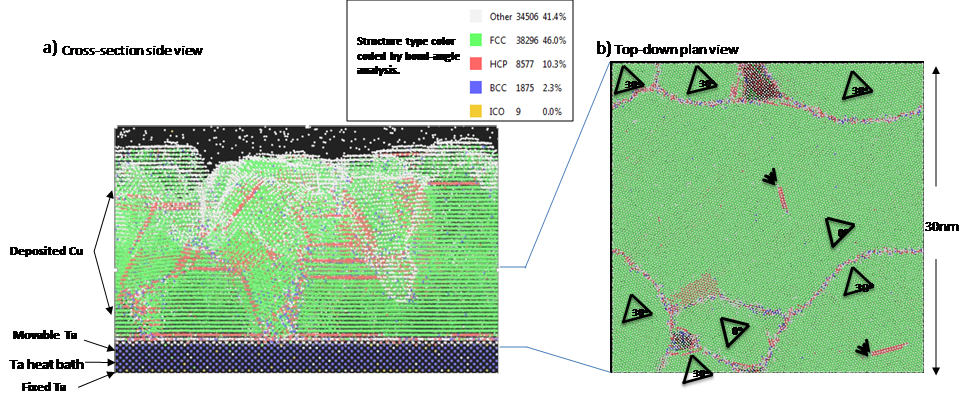
[49, 50] with EAM potentials tuned for binary metal systems. Due to timestep limitations of the MD method, the deposition was simulated at an extremely exaggerated deposition rate (1 adatom/30fsec) at a temperature of 400K in order to get a sufficient thickness of 50 monolayers in the usec timeframe available. Even with the elevated conditions, the resulting (111) FCC grains with 30° rotation were in agreement with experimental reported microstructures[51].


Figure 6.   Cu atoms deposited on a planar Ta substrate a) side-view showing the Ta substrate layers with deposited Cu atoms; b) top-down view of a slice through the substrate and Cu deposited layer showing the microstructural grains, boundaries, and stacking faults.
Multiple instances of these microstructures were then used as input to DFTB transmission calculations to extract the resistivity for grain sizes. Extractions from slices of the realistic planar and trench MD deposition simulations are shown in the datapoints on Figure 5(c), giving good agreement with the analytic extracted curves. It confirms that the analytically generated GB structures are equivalent to the more costly full MD deposited polycrystalline ones, validating the methodology. This shows the power of using a combination of atomistic material modeling tools to generate and analyze microstructural dependence of material properties.
5.   Conclusion
In this paper we briefly reviewed the state-of-the-art of MM in the context of semiconductor TCAD. We showed applications of MM approaches to problems of interest such the interaction of metals at an interface and the effect of metal grain structure on resistance. Before concluding, we would like address two vital aspects of MM. The first is accuracy. With enough effort, i.e.


Figure 7.   Schematic view of material modeling software infrastructure. Downward (blue) arrows show input data flow direction, upward (yellow) arrows show simulation results flow direction.
careful model selection, extensive calibration, vigilance in assuring convergence, MM can often achieve accuracy comparable to experiment. However, this level of effort is not always practical in an industrial setting, nor is it necessary. MM can still be a viable tool for assessing competing technology options provided the simulated trends are physically defensible and consistent with available data for similar systems, even when the absolute value of the results have large error bars.
The second aspect we wish to address is the framework for the ideal MM simulation environment[52]. It starts with having a tool which can create the atomistic structures of the systems we wish to model, as shown in Figure 7. This tool must be able to generate ideal as well as realistic structures, i.e. those with defects and multiple materials. Next we add reliable, highly scalable atomistic simulation code[s] to model the complete system, such as MD, KMC, or DFT and an option to seamlessly exchange atomistic structures between them. Next we would include tools for interatomic potential fitting and verification, and computational utilities for managing massively parallel jobs. To analyze the results, an extended set of postprocessing and visualization options would ideally be encapsulated into a single tool. And finally, the entire system should be connected by a flexible scripting framework, enabling construction of complex simulation flows. With such a system, a monolithic MM system could be used to simulate the majority of problems of interest versus employing individual customized flows for each application, which is the most common approach today.
In closing, we wish to recommend a recently published handbook[53] for further reading.
Acknowledgments
The authors would like to thank the members of Intel’s TCAD, J. Weber, L. Alexandrov, A, Emelyanov for their valuable contributions and discussions, suggesting ideas for MM application examples, and providing simulation results. We are grateful to Dr. Shiuh-Wuu Lee for inviting us to submit this review for publication.
[1] M. Bonitz,Introduction to Computational Methods in Many-Body Physics, Rinton Press Inc, (2006).
[2] E. Strohmaier, et al., “The TOP500 list and progress in High-Performance computing,” Computer48 , 42–49, (2018).
[3] E. Swartz and O. Pohl, “Thermal boundary resistance,” Rev. Mod. Phys.61 (3), 605—668, (1989).
[4] S. Merabia and K. Termentzidis, “Thermal conductance at the interface between crystals using equilibrium and non-equilibrium molecular dynamics,” Phys. Rev. B 86(9), 094303, (2012).
[5] R. O. Jones, “Density functional theory: Its origins, rise to prominence, and future,” Rev. Mod. Phys. 87(3), 897-923, (2015).
[6] A. Abrikosov, L. Gor’kov, and I. Dzyaloshinski, Methods of Quantum Field Theory in Statistical Physics, Dover Publications, (1975).
[7] J.M. Ziman, Electrons and Phonons: The Theory of Transport Phenomena in Solids, OUP Oxford, (2001).
[8] https://en.wikipedia.org/wiki/List_of_quantum_chemistry_and_solid-state_physics_software
[9] C. Freysoldt,et al., “First-principles calculations for point defects in solids,” Rev. Mod. Phys.86 (1), 253-305, (2014).
[10] B. Uberuaga and H. Jonsson, “A Climbing Image Nudged Elastic Band Method for Finding Saddle Points and Minimum Energy Paths,” J. Chem. Phys.113, 9901-9904, (2000).
[11] E. Aprà et al., “NWChem: Past, present, and future,” J. Chem. Phys. 152, 184102 (2020).
[12] S. Plimpton, “Fast parallel algorithms for short-range molecular dynamics,” J. Comput. Phys. 117, 1 (1995).
[13] H. Akinaga and H. Shima, "Resistive Random Access Memory (ReRAM) Based on Metal Oxides," in Proceedings of the IEEE 98 (12), 2237-2251, (2010).
[14] D.A. Drabold, “Topics in the theory of amorphous materials,” Eur. Phys. Jour. B68 (1), 1-21, (2009).
[15] J. Maier and H. Detz, “Atomistic modeling of interfaces in III–V semiconductor superlattices,” Phys. Status Solidi B253, 613-622, (2016).
[16] J. Schneider, et al., “ATK-ForceField: a new generation molecular dynamics software package,” Modelling Simul. Mater. Sci. Eng.25 , 085007, (2017).
[17] G. Hegde, et al., “An environment-dependent semi-empirical tight binding model suitable for electron transport in bulk metals, metal alloys, metallic interfaces, and metallic nanostructures. I. Model and validation,” J. Appl. Phys. 115, 123703 (2014).
[18] N. Zonias, et al., “Large-scale first principles and tight-binding density functional theory calculations on hydrogen-passivated silicon nanorods,” J. Phys.: Condens. Matter22 , 025303, (2010).
[19] M. Luisier, et al., “Atomistic simulation of nanowires in the sp3d5s* tight-binding formalism: From boundary conditions to strain calculations,” Phys. Rev. B74 , 205323 (2006).
[20] J. Hutter, et al., “cp2k: atomistic simulations of condensed matter systems,” Wiley Interdiscip. Rev.: Comput. Mol. Sci. 4, 15–25, (2014).
[21] K. Stokbro K., et al., “Ab-initio Non-Equilibrium Green’s Function Formalism for Calculating Electron Transport in Molecular Devices,” in Introducing Molecular Electronics. Lecture Notes in Physics, Springer, Berlin, Heidelberg, 680, (2006).
[22] Y. Kwok, Y. Zhang, G.-H. Chen, “Time-dependent density functional theory for quantum transport,” Front. Phys.9 (6): 698–710, (2014).
[23] J. Lienig and M. Thiele, Fundamentals of Electromigration-Aware Integrated Circuit Design, Springer, Cham (2018).
[24] Y. Funamizu and K. Watanabe, “Interdiffusion in the Al-Cu System,” Transactions of the Japan Institute of Metals12 (3), 147-152, (1971).
[25] C. Li et al., “Molecular dynamics simulation of diffusion bonding of Al–Cu interface,” Modelling Simul. Mater. Sci. Eng.22 (6), 065013 (2014).
[26] M. Zaenudin, et al., "Study the Effect of Temperature on the Diffusion Bonding of Cu-Al by Using Molecular Dynamics Simulation," 2019 IEEE International Conference on Automatic Control and Intelligent Systems (I2CACIS), Selangor, Malaysia, pp. 345-348, (2019).
[27] F. Zahid, et al., “Resistivity of thin Cu films coated with Ta, Ti, Ru, Al, and Pd barrier layers from first principles,” Phys. Rev. B, 81, 045406, (2010).
[28] T.B. Massalski, et al., “Binary Alloy Phase Diagrams,” Ed. 2, ASM International, (1990).
[29] https://www.asminternational.org/home/-/journal_content/56/10192/15469013/DATABASE
[30] M. Griebel, et al., “Numerical Simulation in Molecular Dynamics,” in Texts in Computational Science and Engineering, Springer-Verlag Berlin Heidelberg, 5, (2007).
[31] S. Foiles and M. Baskes, “Contributions of the embedded-atom method to materials science and engineering,” MRS Bulletin 37(5), 485-491, (2012).
[32] T. E. Oliphant, “Python for Scientific Computing,” Computing in Science & Engineering 9, 10-20 (2007).
[33] H. Mehrer, “Diffusion in Solids,” in Springer Series in Solid-State Sciences, Springer-Verlag Berlin Heidelberg, 151 (2007).
[34] A.B. Bortz, M.H. Kalos, J.L. Lebowitz, “A new algorithm for Monte Carlo simulation of Ising spin systems,” J. Comp. Phys. 7(1), 10-18, (1975).
[35] https://spparks.sandia.gov/index.html
[36] R. Weinkamera, yet al., “Using Kinetic Monte Carlo Simulations to Study Phase Separation in Alloys,” Phase Transitions 77(5-7), 433–456, (2004).
[37] N. Metropolis et al., “Equations of state calculations by fast computing machine,” J. Chem. Phys. 21(6), 1087-1091 (1953).
[38] A. Stukowski, “Visualization and analysis of atomistic simulation data with OVITO–the Open Visualization Tool,” Modelling Simul. Mater. Sci. Eng. 18, 015012, (2010).
[39] G. Henkelman and H. Jo´nsson, “Long time scale kinetic Monte Carlo simulations without lattice approximation and predefined event table,” J. of Chem. Phys. 15(21), 9657- 9666, (2001).
[40] L. K. Beland, et al., “Kinetic activation-relaxation technique,” Phys. Rev. E 84, 046704 (2011).
[41] B. Puchala, M. L. Falk, and K. Garikipati, “An energy basin finding algorithm for kinetic Monte Carlo acceleration,” J. Chem. Phys. 132, 134104, (2010).
[42] A. Chatterjee and D. G. Vlachos, “An overview of spatial microscopic and accelerated kinetic Monte Carlo methods,” J. Computer-Aided Mater. Des. 14, 253–308, (2007).
[43] J.-F. Joly, et al., “Optimization of the Kinetic Activation-Relaxation Technique, an off-lattice and self-learning kinetic Monte-Carlo method,” J. of Phys.: Conference Series 341, 012007, (2012).
[44] J. Cai and Y. Y. Ye, “Simple analytical embedded-atom-potential model including a long-range force for fcc metals and their alloys,” Phys Rev B 54, 8398-8410 (1996).
[45] G. Stefanucci and R. Van Leeuwen, “Nonequilibrium Many-Body Theory of Quantum Systems: A Modern Introduction,” Cambridge University Press (2013).
[46] X.G. Zhang, Kalman Varga, Sokrates T. Pantelides, “Generalized Bloch theorem for complex periodic potentials: A powerful application to quantum transport calculations” Phys. Rev. B76 , 035108 (2007).
[47] P. Koskinen and V. Makinen, “Density-Functional Tight-Binding for Beginner,s” Computational Materials Science, 47(1), (2009).
[48] D. A. Papaconstantopoulos, “Handbook of the Band Structure of Elemental Solids,” Springer (2015).
[49] X. W. Zhou and E. B. Webb III, “Atomically Engineering Cu/Ta Interfaces” Sandia Report SAND2007-5941, (2007)
[50] M. F. Francis, et al., “Atomic assembly of Cu/Ta mulitlayers: Surface roughness, grain structure, misfit dislocations, and amorphization” Journal of Applied Physics 104, 034310 (2008)
[51] J. S. Chawla, et al., “Electron scattering at surfaces and grain boundaries in Cu thin films and wires” Phys Rev B 84, 235423 (2011)
[52] D. Mejia et al., “NemoViz: a visual interactive system for atomistic simulations design,” Visualization in Engineering 6 , 6 (2018)
[53] “Handbook of Materials Modeling,” W. Andreoni and S. Yip, Ed., Springer International Publishing, (2018).
Article and author information
Boris A. Voinov
Boris A. Voinov received the M.S. degree from the Moscow Institute of Physical Engineering, in 1979, the Ph.D. degree from the State Nuclear Research Center – Institute of Experimental Physics (VNIIEF), Sarov, Russian Federation in 1989. He has been with VNIIEF from 1980 to 2003 as a Senior Research Scientist focused on theoretical, computational, and applied researches in solid state, plasma kinetics, radiation transfer, wave generation and propagation. In 2003 he joined TCAD at the Logic Technology Development, Intel Corporation.
Patrick H. Keys
Patrick Keys is a senior TCAD engineer at Intel Corp. He has almost 20 years of experience developing internal process modeling software and working closely with process integration teams to develop next generation transistor technologies. He holds numerous technology patents. Patrick received his B.S. degree in electronics engineering from the Univ. of Scranton, PA, a M.S. degree in Materials Science & Engr. from New Jersey Institute of Technology (NJIT), and Ph.D. in Materials Science & Engr. from the University of Florida.
Stephen M. Cea
Stephen Cea received the B.S. degree in electrical engineering from the University of New Hampshire, Durham, in 1990, and the M.S. and Ph.D. degrees in electrical engineering from the University of Florida, Gainesville, in 1993 and 1996, respectively. In 1996, he joined the TCAD Department, Intel Corporation, Hillsboro OR. He currently manages the Device and Process Modeling Group, TCAD Department, Intel Corporation, Hillsboro, OR. He has published over 20 works in refereed journals and conferences and holds greater than 25 patents.
Ananth P. Kaushik
Mark A. Stettler
Mark A. Stettler is Vice President in Technology Development and the Director of Computational and Modeling Technology at Intel Corporation. He has 5 issued patents and more than 40 publications in the field of semiconductor device modeling and process development. Mark earned a B.S. in electrical engineering from the University of Notre Dame. He also holds a master’s degree and a Ph.D. in electrical engineering, both from Purdue University.
Publication records
Published: Dec. 30, 2020 (Versions2
References
Journal of Microelectronic Manufacturing