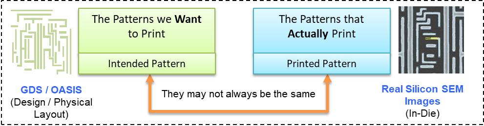
Research Article Current Issue Versions 2 Vol 3 (4) : 20030410 2020
Download
Pattern-Centric Computational System for Logic and Memory Manufacturing and Process Technology Development
: 2020 - 09 - 18
: 2020 - 11 - 02
: 2020 - 12 - 30
2040 78 0
Abstract & Keywords
Abstract: Chip designers employ computer-aided design, circuit simulation, and design rule check systems. Lithography engineers employ model-based OPC (Optical Proximity Correction) and model-based print-simulation systems. Reticle inspection teams employ Aerial Image Measurement Systems® and Virtual Stepper® Systems. These teams are accustomed to evaluating and deploying state-of-the-art computational systems. When real-silicon fabrication begins, however, the teams responsible for line monitoring, wafer inspection, and yield attainment operate without the benefit of similarly advanced computational systems. In this paper we describe such a system and explore its applications and benefits. The system has received three U.S. patents [1,2,3] and brings together the significant potential of CAD (Computer Aided Design) layout (GDS, OASIS), Die-to-Database, and Machine Learning to build a dynamic, self-improving computational system. Featuring care area generation, advanced machine learning-based SEM (Scanning Electron Microscope) sampling that optimizes both DOI (Defect of Interest) capture rate and discovery of new defect types, comprehensive extraction of all Information of Interest(IOI) from all SEM images, detection of defect types not possible before, massive pattern fidelity analysis, full chip pattern decomposition and risk scoring via machine learning, innovative PWQ (Process Window Qualification) analysis and process window determination, risk assessment of new tape-outs, large scale in-wafer OPC verification and more, the system delivers a comprehensive pattern centric platform for process technology development and manufacturing.
Keywords: Die-to-Database; Full Chip Decomposition; Machine Learning; Defect Discovery; Pattern Fidelity; Pattern Risk Scoring; OPC Verification; Process Window Qualification
1.   Introduction
At every major technology node, the density of transistors per unit area approximately doubles, and so does the quantity of raw data that fabs need to extract, track, and analyze. Compounding the problem is the fact that doubling the density of transistors means shrinking their size. Not only are smaller geometries harder to fabricate, they are harder to inspect. The semiconductor industry has witnessed a rapid progression of technology nodes thanks to advancements in lithography such as ArF Immersion and EUV (Extreme Ultra Violet wavelength), and attendant advancements in material stacks. These advancements have precipitated advancements in adjacent areas. For the areas of wafer inspection, line monitoring and yield enhancement, adjacent advancements have been made in E-Beam (electron beam) and SEM technologies that have the ability to detect and resolve increasingly smaller deviations in increasingly smaller geometries – and at relatively higher speeds. However, these tools are still throughput-limited and fabs continue to employ a combination of (a) high-speed low-resolution optical tools and (b) low-speed high-resolution E-Beam and SEM tools.
Driven by market and technology demands, leading manufacturers of E-Beam and SEM tools are investing aggressively in new technologies such as faster single-beam systems (that feature larger spot sizes while retaining high resolutions) and multi-beam systems to confront the continuing challenges of throughput and coverage. But hardware alone is not sufficient for yield learning and line monitoring. Hardware generates raw data, but not information. Software generates information and, more importantly, actionable information.
In this paper we present a pattern-centric computational system for the fab that leverages the fields of CAD layout (GDS/OASIS), Die-to-Database, and Machine Learning to enable bold new opportunities for wafer inspection, SEM review, defect discovery, (Focus Exposure Matrix) FEM/PWQ analysis, Litho/OPC optimization, pattern fidelity monitoring, yield prediction and risk assessment (especially for new tape-outs), and more. We begin with a brief discussion of the technology before focusing on value-added applications.
2.   Building a Pattern Centric Computational System
Because the essential task of a semiconductor wafer fab is to print patterns onto the wafer, Anchor’s computational system is designed to be pattern centric. The CAD layout is a database of patterns. OPC is performed on patterns. Mask writers etch patterns (contained in MEBES files). Lithography process windows are determined using FEM/PWQ techniques that analyze patterns in each focus/exposure modulation. Test chips are composed of a diversity of patterns. DFM (Design for Manufacturing) databases record weak patterns. DRC (Design Rule Check) rule decks are designed to avoid problematic pattern layouts.
Patterns are indeed essential components. But the notion of patterns takes a back seat in the operation of the wafer fab. This is not necessarily desirable, but it is understandable because (a) the design house is CAD based, (b) the OPC team is CAD based, and (c) the mask house is CAD based. But not the fab. Once the reticle or mask enters the fab, the digital side of manufacturing is essentially complete (where every digital “run” produces identical results), and the analog side begins (where every analog “run” produces slightly different results). Like snowflakes, no two wafers nor any two die are exactly alike. There are differences every time the wafer is exposed or developed or etched or planarized or implanted or cleaned. The process steps leading from the front end of line to the back end of line are analog steps.
For a fab operating in the analog domain to communicate and coordinate more effectively with the Design, OPC and Mask teams that operate in the digital domain, it needs to adopt the language of patterns as well.
For years, fabs have struggled to cope with patterns, often spending days or weeks of manual effort to analyze large quantities of FEM/PWQ results, for example, and provide actionable information to the OPC team or to appropriate process modules.
Anchor’s computational system arises from the intersection of the two primary domains of intended and printed patterns shown in Figure 1, and consists of three pillars:
1.Printed Pattern Database2.Design Decomposition Database3.Machine Learning


Figure 1.   Intended Patterns are represented in the CAD Layout, and Printed Patterns are represented in SEM images, from which the Printed Pattern Database is built.
3.   Three Pillars of a Computational System for the Fab
The CAD layout is a golden reference database of the intended patterns. Over the past decade and a half, use of CAD inside the fab has enabled new opportunities for yield analysis and wafer inspection. But is there an analog equivalent of the CAD layout? That is, is there a database of the printed patterns?
As shown in Figure 2, if a database of printed patterns were to exist, it could once again enable new opportunities for process technology development and manufacturing. We call this the Printed Pattern Database, and it is the most fundamental of the three pillars of Anchor’s computational system.


Figure 2.   Three Pillars of Anchor's Computational System.
The printed pattern database is constructed in an intelligent manner that extracts and retains only the patterns of interest within each SEM image. Patterns of interest are identified by a set of parametric search rules that operate in real time on each image. Once extracted, each pattern of interest is assigned a class code corresponding to the rule that identified the pattern. For example, when a tip-to-line pattern is found, it is classified as a tip-to-line. When a tip-to-tip pattern is found, it is classified as a tip-to-tip. This enables the user to query and study the yield impacts of specific types of patterns along with the variations of those patterns (e.g. study the differences in printability of tip-to-line patterns as a function of the gap between tip and line).
The Design Decomposition Database is the next pillar. Each layer of interest in the CAD Layout is decomposed systematically into a collection of unique constituent patterns of a specified maximum size. A poly layer, for instance, will be fully decomposed into its unique constituent patterns.
Decomposition is performed using the same parametric rule engine that builds the printed pattern database, which means that only patterns of interest are extracted when decomposing the full chip layout. This eliminates don’t care patterns that would otherwise burden the database with too many nuisance patterns. When a layer is fully decomposed into its constituent patterns of interest, the result is an abbreviated representation of the layer.
The third pillar, machine learning, bridges the first two pillars and enables entirely new opportunities for yield learning and process optimization.
There are at least two ways to model a real-world system in order to make specific kinds of predictions. The conventional method is to build the model from first principles and tune the model until it begins to make sufficiently accurate predictions. This is done, for example, with OPC Simulation where selected properties of light waves, optics, and materials are combined into a mathematical model that takes a CAD layout (post-OPC layout) as input and generates a simulated print (contours) as output [4,5,6 ]. Unfortunately, such models have considerably expensive development, optimization, and run-time requirements.
The alternative method is to allow a computer to build the model itself using appropriate training data that provide sufficient examples of if this goes in, then that comes out. The computer examines all of the inputs and their expected outputs and builds a self-learning model that can take a new input not seen before and infer or predict the output. Anchor’s computational system applies this idea in many ways, one of which is to learn from the Printed Pattern Database and assess the printability risk of all patterns in the Design Decomposition Database.
The Printed Pattern Database (PPD) provides exactly the training set necessary for Machine Learning because it contains both the (a) intended pattern (in CAD database) and the (b) printed pattern (on die). This provides a rich training set because it contains numerous examples of if this goes in (the intended pattern), then that comes out (the printed pattern). New SEM images that are continuously being captured by the fab are added to the PPD. This dynamic environment allows the machine learning system to learn continuously and therefore improve its prediction accuracy. As the accuracy of the machine improves over time, the system moves closer to an expert system.
4.   Value-Added Applications
Numerous value-added applications are enabled by the three pillars of Anchor’s pattern centric computational system. We discuss a handful of those applications at an introductory level in order to keep this paper reasonable in size.
4.1. Care Area Generation for Optical and E-Beam Inspection
Optical inspection tools are still essential because of their high throughput and high wafer coverage. Although they lack the resolving power of an E-Beam tool, they incorporate advanced features such as KLA’s NanoPoint® / PinPoint® and Applied Materials’ Marker® that attempt to improve sensitivity to defects by reducing a particular type of system noise [7, 8]. To make use of these features, it is first necessary to perform full-layer pattern segmentation such that the patterns in each segment are relatively homogeneous. Inspection recipes can be optimized for each segment, thereby improving sensitivity in each segment, shown in Figure 3.


Figure 3.   Noise characteristics of conventional care areas on the left may contain undetectable defects because they are buried below the noise floor. More homogeneous care areas result in less noise (right) within each care area group, allowing previously hidden defects (green) to rise above the noise floor and be detected.
Anchor’s Design Decomposition Database (DDD), with its ranked collection of patterns, enables this segmentation in a manner not possible before. High-risk patterns from the DDD are first placed into “look-alike” groups such that the patterns within each group are relatively homogenous. Then each look-alike group is exploded, which means that all instance locations of all member patterns are added to the group. Now each group contains a set of look-alike patterns and every location on the die where those patterns occur. Each group becomes a “segment” for a KLA or Applied Materials inspection tool. These segments, consisting of relatively high-risk patterns, can be inspected with high sensitivity without incurring high noise.
E-Beam inspection tools are playing an increasing central role because of their ability to resolve tiny details on leading edge technology nodes. Although they lack speed and provide limited wafer coverage, advancements are being made to both speed and resolution. For any low-throughput tool, choosing the right care areas is of paramount importance. High risk patterns in the Design Decomposition Database are used to supplement a fab’s existing E-Beam care area.
4.2.   Review SEM Sample Plan
Review SEMs have been used for decades to compensate for a lack of resolution on optical inspection tools. The patch images they produce are pixelated and cannot be used to adequately scrutinize the properties of every defect. A clear and detailed image of the defect is necessary to determine its type, its shape, its causal mechanism, and its impact to yield (killer versus non-killer).
Because of the relatively slow throughput of Review SEM tools, it is necessary to pick a subset of the defects that were detected by the optical inspector. If a poor subset is picked or sampled, not much is learned. Fabs generally expect the sampled subset to (a) contain as many known defects of interest (DOI) as possible and (b) discover new defect types. It may seem straightforward to generate a sample plan that addresses both needs, but these are often competing requirements. If the sample plan is biased too much around (a), it will lose its ability to discover new defect types (b), and vice-versa.
Given a sampling budget of N defects for SEM review, Anchor’s computational system generates a balanced sample plan while providing users the ability to bias the algorithm a little in either direction. Balancing the sample plan means choosing defects from the original population whose extended properties are likely to both (a) increase capture rate of known DOI and (b) discover new defect types. In broad terms, Anchor’s computational system derives these extended properties and creates a final sample plan through a combination of supplied defect properties, generation of new properties through reprocessing of patch images, and machine learning.
The computational system offers an additional option to apply pattern risk scores that are stored in the Design Decomposition Database. Sample plan candidates can be further filtered in or out based on their pattern risk scores.
4.3. Comprehensive Extraction of Information of Interest(IOI) from SEM Images
Despite the paramount importance of high-resolution SEM images at all technology nodes, and especially the leading technology nodes, they are predominantly wasted. At sub-14nm nodes in particular, each SEM image contains large amounts of information, but conventional workflows examine only the center of each image to classify a defect that is expected to be present in the center. Unfortunately, upwards of 50% to 70% of SEM images do not contain a “SEM visible” defect in the center. It is likely that some sort of anomaly is indeed present in the center because the optical column in the wafer inspection tool registered an anomaly. But a SEM tool is not an optical tool; the mechanics of electron beam emission and scatter are sufficiently different from the mechanics of photon emission, transmission, and reflection. So, a SEM tool is physically unable to see certain types of optical defects, and these are referred to as SEM Non-Visuals or SNVs.
When we consider the low throughput of a SEM tool, the limited number of images that the fab’s cycle time allows, and the paramount importance of the SEM for yield learning, it is profoundly disconcerting to realize that 50% to 70% of SEM images are simply discarded for being SNV and the remaining ones are examined in a superficial manner (i.e., the center portion of the image is examined for the presence of a defect, and the defect is classified). The type of information that is most effective for yield learning also happens to be the information that is most often discarded.
Anchor’s Printed Pattern Database and value-added applications eliminate that waste.
Every SEM image, regardless of SNV status, is analyzed from head to toe. As shown in Figure 4, every bit of Information of Interest (IOI) is extracted and recorded in the Printed Pattern Database for the value-added applications to exploit. Parametric pattern search rules are invoked on each image to find and extract Information of Interest while rejecting don’t care features. Information of Interest includes named patterns of interest and their measurements. For example, a named pattern might be a tip-to-line or a comb or a line end with single via or a set of dense thin lines, etc. Their measurements will indicate how well or how poorly each named pattern is printing – in effect, this enables pattern fidelity monitoring and analysis.
Each SEM image is also checked for the presence of any number of predefined defect types such as hard breaks and bridges, soft breaks and bridges, line end pullback with exposed vias, misshapen contacts and vias, etc. Conventional workflows look for one defect per image (1-to-1), but Anchor’s computational system looks for all defects on each image (1-to-many). As we discuss later, Anchor’s die-to-database approach for defect detection enables new types of defects to be detected.


Figure 4.   All Information of Interest Extracted from SEM Image. The image is scanned for both defects (left) and patterns-of-interest (right). All defects are classified and reported; and all patterns-of-interest are measured and tracked in the Printed Pattern Database.
4.4. Detection / Discovery of Defect Types not Possible or Practical Before
Conventional defect detection methods rely on target-die to reference-die comparison where the reference die may be adjacent to the target die or it may be a preselected golden die. There are several limitations with this approach that prevent certain categories of defects from being detected and corrected, leading to diminished yields and extended process debug cycles. Here we list some of the defect types that are either impractical or impossible to detect using conventional methods, but which are fully detected by Anchor’s pattern centric computational system. Some of the examples in the ensuing subsections will refer to the representative cross-section shown in Figure 5.


Figure 5.   Representative cross-section of FinFET device.
4.4.1.   CA to CB Bridge (Short)
CA and CB structures are part of the same contact layer, but they connect to different functional elements of the transistor. CA connects to source and drain, but CB connects to poly (PC). Variations in the patterning process for contact layers may result in undesirable bridging between CA and CB structures. This bridging could be the result of marginalities in (a) design, (b) lithography, or (c) etch. Without the chip design serving as the reference, it is impractical for yield engineering to distinguish between CA and CB in images where only the contact layer is visible. Cross sectional analysis may be needed to positively distinguish CA from CB because such an analysis reveals the under or previous layer to which each contact is connected. Anchor’s pattern-centric approach, however, can readily detect CA-CB bridges and distinguish them from CA-CA and CB-CB bridges, as shown in Figure 6.


Figure 6.   Design layout for Contact layers CA/CB (left) and Representative SEM image for Contact layer features (right).
4.4.2. Line End Pullback Leading to Exposed VIA/Potential VIA Disconnection (Open)
The manner in which a wafer inspection recipe is tuned or optimized can result in either a significant under-detection or over-detection of line-end pullbacks. Detection of pullbacks is essential, but not all pullbacks are killer defects or otherwise consequential. Pullbacks that are consequential cannot be differentiated from the entire set of pullbacks because conventional defect detection methodologies lack a comprehensive reference image from which such determinations can be made. D2DB-PM, however, uses the comprehensive chip design as its reference, and is therefore able to detect additional categories of defects such as ‘line-end pullback with exposed under layer via’ and ‘line-end pullback with future exposed upper layer via’ that will result in an electrical disconnect or increased resistivity, as shown in Figure 7.


Figure 7.   Target design for V0-M1-V1 overlay (left) and Representative M1 contour with design overlay. Exaggerated line-end pullback on both ends for discussion purposes (right).
4.4.3.   Cut Layer Issues (Short, Open)
Cut Masks are commonly used in advanced nodes to assist in printing of short lines with narrow gaps, as explained in Figure 8. This widely adopted method prints long lines and then cuts them into the desired lengths with a subsequent cut mask. But the placement or overlay of the cut mask atop the previous layer is not always optimized and may render unwanted artifacts and errors on the wafer. Without access to a comprehensive reference image, conventional defect detection methodologies are unable to (a) detect all such defects and (b) to do so reliably every time.


Figure 8   Target PC feature with Cut Mask (left) and Representative SEM image after cut or CT (right).
4.4.4.   Extra Pattern Detection
Extra features are sometimes produced inadvertently during the patterning of repeated structures. This is often seen in FIN and VIA layers. Conventional Die-to-Die detection methods are undependable because more than one die may have this issue. Anchor’s computational system can reliably detect extra patterns because the chip design serves as the reliable reference, shown in Figure 9. This approach is also used to detect any extra feature on wafer caused by residue or fall-on particle.


Figure 9.   Target FIN feature (left) and Representative SEM image (right).
4.4.5. Hole Analysis (Size Variation, Short, Missing)
Contacts and vias (i.e. holes) are printed by the billions on large logic devices, and by the hundreds of billions on each wafer at each hole layer. They play an essential role in the routing of electrical signals between layers. However, there can be considerable variation in the printing of holes. Variations can arise from natural process drift, from proximity effects of neighboring clusters, from randomness in the material and topography, from etch chamber control, etc.
Anchor’s computational system monitors hole size and shape, detects various types of shrinkages and enlargements, and identifies missing holes, as shown in Figure 10. Moreover, it can automatically identify all holes in an image and analyze each one, leading to exceptionally thorough analysis.


Figure 10.   Hole defect detection.
4.5.   Massive Pattern Fidelity Analysis
Pattern fidelity – not just defectivity – has always been of importance to the fab, but fidelity monitoring has been limited to low-frequency, time-consuming CD-SEM (Critical Dimension Scanning Electron Microscope) measurements [9,10]. CD-SEMs continue to play an important role in accurately measuring features from both orthogonal and oblique angles. These measurements are typically performed on preselected features on designated wafers.
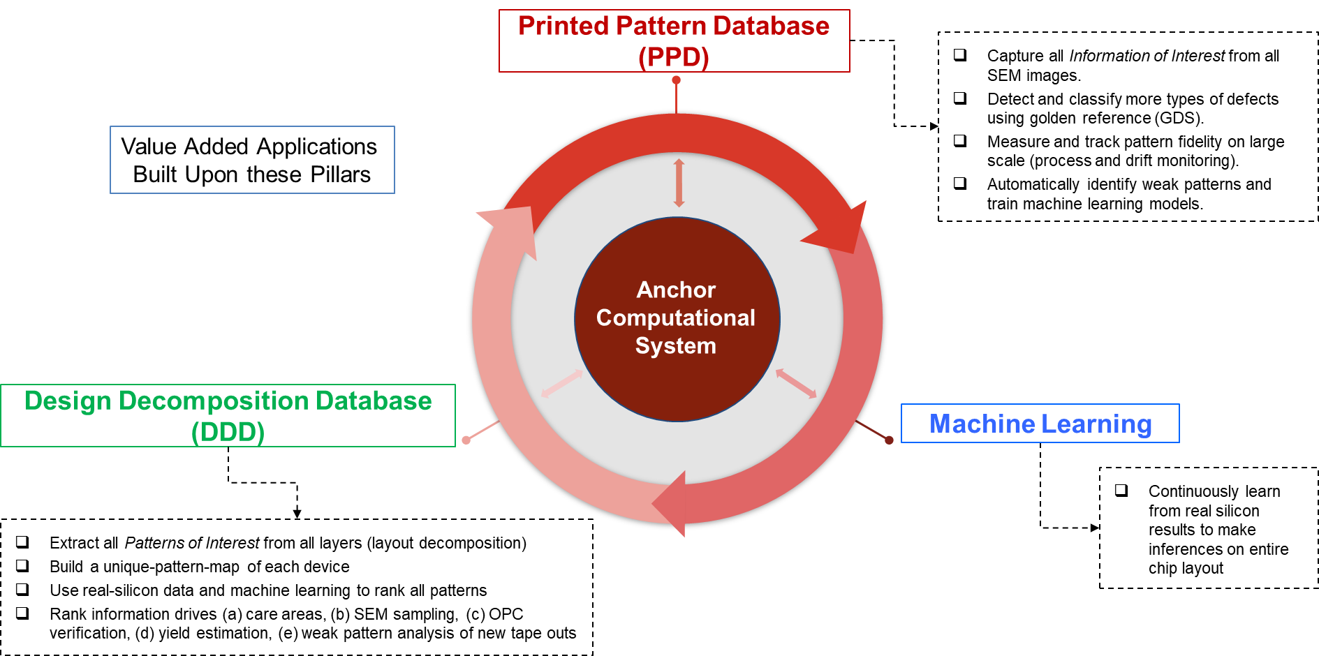
Anchor’s computational system reimagines the concept and deploys it on a massive scale on all wafers and on all features for which there are Review SEM images. The line itself is monitored not only for the traditional concept of defect, but also for the concept of pattern fidelity, which is in effect a “CD”-type measurement, but without the same level of measurement accuracy as a calibrated CD-SEM measurement. As such, inline continuous massive pattern fidelity measurement supplements the conventional CD-SEM operation [11]. It has the potential to provide much earlier warnings of pending problems by tracking changes or trends in pattern fidelity before they become bona fide defects. At the leading technology nodes, even small changes in pattern fidelity lead to significant electrical parasitics or parametric issues. A resistive via, for instance, may be caused by a slightly narrow and therefore partially blocked via that can impact device timing characteristics, produce single bit failures in memory devices, and produce various other parametric problems. Line thinning, line edge roughness, corner rounding, corner-to-corner artifacts, etc. are all liable to cause parametric issues.
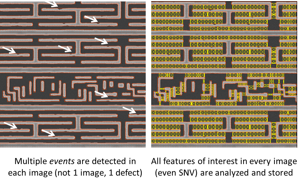
Anchor’s computational system performs massive pattern fidelity analysis on each image, but does so in a pattern-centric manner that searches each aligned SEM image for all patterns of interest or POI, measures their printed dimensions, compares them against the reference design, and stores all results in the Printed Pattern Database.
Patterns-of-interest (POI) are based on one or more parametric search rules. POI can also be identified automatically from the Design Decomposition Database by searching for patterns with high risk scores. Here we provide an example based on parametric search. Tip-to-line is a common pattern-of-interest, in which the amount of gap between tip and line (among other parameters) may affect printability or pattern fidelity.
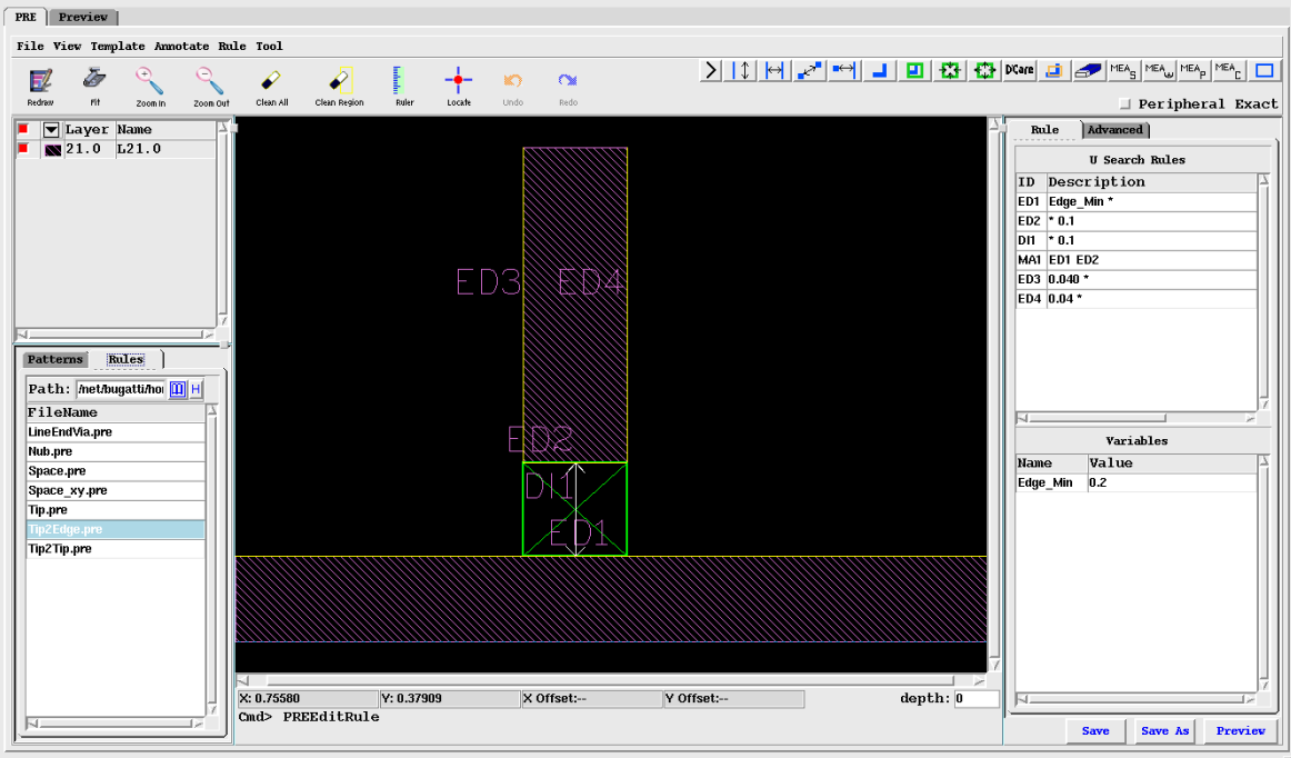
In the example shown in Figure 11, we use a graphical user interface (GUI) to create a tip-to-line rule. We specify several constraints such as the maximum width of the tip, the minimum length of the tip, and the maximum gap between tip and line. We want the rule to match tips whose widths are less than 100nm, whose lengths are at least 40nm, and the gap is at most 100nm.


Figure 11.   
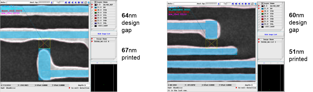
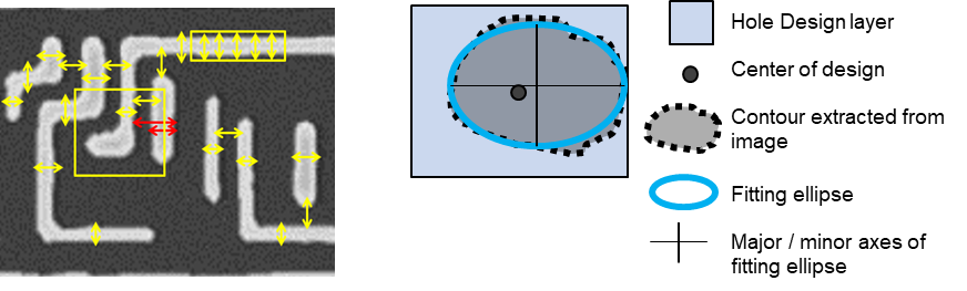
Defining Tip-to-Line Rule with Parameters (Constraints).
This single rule will match all variations of tip-to-line where the tip width is less than 100nm, the tip length is greater than 40nm, and the gap is less than 100nm. When we run this rule against the two sample SEM images shown in Figure 12, we find a match where the reference tip-to-line gap (from design) is 64nm and another where the reference gap is 60nm. Once these patterns of interest (in blue) have been found, their printed sizes are measured either (a) from the image itself or (b) from the extracted contour. In the first example, the measured value is 67nm, and in the second, the measured value is 51nm.


Figure 12.   Two variations of tip-to-line matched by the parametric search rule.
Because each SEM image is scanned from top to bottom, there might be tens or hundreds of matching patterns on each image. From a small set of sample images, we obtained the result as shown in Figure 13.
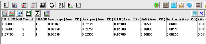

Figure 13.   Sample measurement results of tip-to-line.
In column 1 we see that the tip-to-line rule found 3 variations of the pattern:
Variation 1: Reference gap 60nm. Average of the printed gap was 58.67nm
Variation 2: Reference gap 64nm. Average of the printed gap was 61.50nm
Variation 3: Reference gap 71nm. Average of the printed gap was 62.50nm
Litho/OPC and process engineers can examine this table to study the effects of gap size on the overall fidelity of the printed pattern. They can ask questions such as if the design or reference gap is reduced to X, how will that affect the printability of the pattern? Similarly, if the design or reference gap is enlarged to Y, how will that affect the printability of the pattern? In other words, the effects of specific variations in the physical layout can be studied in a comprehensive manner.
This example also demonstrates the value of speaking the universal language of patterns. There are more examples shown in Figure 14 that demonstrate the potential of SEM images to reveal detailed analysis of process variation. Anchor’s computation system is like an “analog to digital” converter – it converts the rich information content of analog SEM images into concise digital design patterns while retaining all of the information associated with the analog print.
When we expand the example by using (a) multiple parametric search rules and (b) hundreds or thousands of SEM images, we obtain a deep understanding of the process and its limitations. For (a) each pattern type (e.g. tip-to-line, tip-to-tip, etc.) and (b) each variation of each pattern type (e.g. tip-to-line gaps of 60nm, 64nm, 71nm, etc.) we create a Box Plot that represents all of the measurements of that particular pattern variation. For instance, if we found and measured fifty tip-to-line patterns with intended gap of 60nm, we create a box plot that shows how close or how wide apart all of the individual measurements were, and how much those measurements deviated from the reference of 60nm.


Figure 14.   
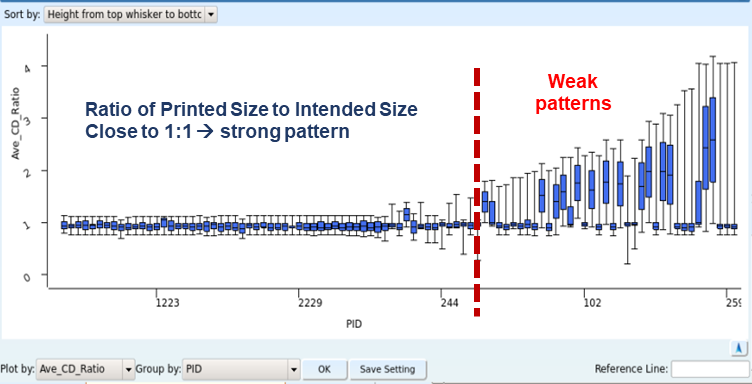
Additional examples of various features being measured.
If we do the same for all patterns and their variations, we end up with a box plot as shown below. Each box represents the measurements of one specific pattern (e.g. tip-to-line with reference gap of 60nm). In this example we see numerous patterns.


Figure 15.   Box Plot of Various Patterns as a Function of the Ratio of Printed Pattern Measurement to Intended Pattern Measurement. Values closer to 1:1 indicate strong patterns.
Each box in a box plot shows several statistics about each specific pattern: the average and median values of all measurements, the range where most of the values are clustered, and outliers. It is a particularly effective way to identify weak and strong patterns, as shown in Figure 15. This particular box plot is based on the ratio of measured value to intended value. If the ratio is 1:1, it indicates a strong pattern because the measured values of all instances of that pattern matched the intended value. The more a box diverges from 1:1, the weaker the pattern. In this chart we see that the left half of patterns are printing well, with ratios close to 1, but the right half diverges significantly, indicating progressively weaker patterns. This automatically separates weak patterns from strong patterns, providing actionable information for root cause analysis.
Although this chart shows a large collection of patterns, we can track the behavior of individual patterns as well. Given a particular pattern A, we can:
Build a box plot of its measurements by time and track the fidelity of pattern A day-by-day or week-by-week or before-and-after a mask or process revision.
Build a box plot of its measurements sorted by process tool ID (e.g. scanner 1 or scanner 2, or etcher 1 or etcher 2, or chamber 1 or chamber 2) for (a) tool matching purposes, (b) identification of problematic tool or chamber, or (c) process drift monitoring.
Build a box plot of its measurements by Focus / Exposure modulation on an PWQ or FEM wafer to study the subtle changes in the behavior of pattern A across F/E modulations. (See next section.)
4.6. Innovative FEM/PWQ Analysis and Process Window Determination
Lithography process window determination is a critical step in the setup and tuning of a scanner recipe. Two of the most significant recipe parameters are (a) focus offset and (b) exposure dose. Different patterns and different neighborhoods of those patterns are affected differently by focus and exposure settings, which are determined by exposing a reticle or mask using a series of focus and exposure modulations and analyzing the results of each modulation.
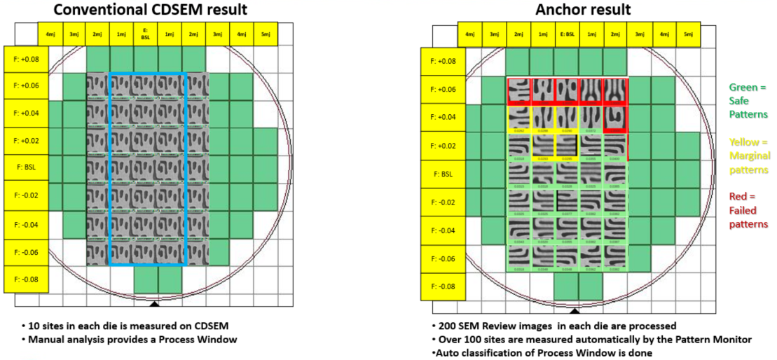

Figure 16.   Conventional vs Anchor FEM Analysis [12].
The conventional method of analyzing Focus/Exposure Modulations (FEM) is by performing a high-sensitivity wafer inspection followed by a large SEM Review in which tens of thousands of SEM images are captured and analyzed for the presence of hard defects. The conventional method does not take pattern fidelity into account and therefore cannot track or report the subtle deviations that occur on each pattern across each modulation. Subtle deviations – pattern fidelity variations – are playing an increasingly significant role in parametric yield loss. Establishing a lithography process window that takes into account pattern fidelity (not just pattern defectivity) leads to a more robust result [12,13,14,15]. A side-by-side comparison of the process window map obtained by conventional method and by Anchor’s method is shown in Figure 16. Anchor’s computational system redefines and reinvents FEM/PWQ analysis in the following ways:
The computational system checks every SEM image for the presence of die-to-database defects. Some of these defects are not detectable using conventional die-to-die or die-to-golden die techniques. Multiple defects can be detected on a single image.
The computational system measures every feature of interest in every SEM image (massive metrology) to generate pattern uniformity statistics for each pattern of interest. This enables pattern fidelity analysis.
The computational system tracks the uniformity of like patterns across each modulation to generate Bossung Curves automatically for hundreds or thousands or tens of thousands of patterns. These Bossung Curves supplement – not replace – conventional CD-SEM analysis because accuracy of measurements from Review SEM is limited. Nevertheless, these Bossung Curves are produced more quickly and cover a significantly wider set of patterns. They provide valuable early feedback.
The combination of (a) better defect detection, (b) pattern uniformity/fidelity analysis, and (c) generation of Bossung Curves for a wide set of patterns results in the reinvention of PWQ/FEM analysis.
4.7.   Risk Assessment of New Tape-outs
Historically, it has been difficult to comprehensively assess the yield risk of a new incoming device. This requires the device to be searched for known weak patterns in order for corrective action to be taken by Litho/OPC teams before the mask is made.
The Design Decomposition Database, in which all patterns of interest are ranked by a machine learning model built from real printed wafer images, enables comprehensive full-chip pattern risk assessment for new tape-outs. The new tape-out is decomposed into constituent patterns that are both (a) cross-referenced with existing patterns in the Design Decomposition Database and (b) assigned risk scores directly by the trained machine learning model. The new tape-out, therefore, is systematically evaluated for potential risk, and corrective action can be taken well in advance of printing the (expensive) masks.
4.8.   Large Scale in-wafer OPC Verification
OPC simulations are standard practice in most fabs. They are based on complex and finely tuned models of the lithography column, and often take hours or days to run on a large cluster of computing nodes (servers). OPC simulations produce a report that grades the lithography risk of each pattern (including the neighborhood in which the pattern lies). Some patterns are clearly marked “weak”, others are “borderline weak”, and others might be “unknown”.
An OPC result is a set of patterns and their risk assessments. But these patterns are very difficult to verify in the fab because once the reticle is printed, a digital-to-analog conversion has taken place. SEM images are analog bitmaps, and these images cannot be compared directly with the OPC simulation results. Instead, images (analog) must be converted back to patterns (digital). This analog-to-digital conversion is once again the basis for Anchor’s pattern-centric computational system. It allows thousands or millions of SEM images to be converted back into digital (pattern) representations that can finally be compared with OPC simulation results in a comprehensive manner to assess the validity of the OPC model. Specifically, we can answer such questions as:
If OPC simulation predicted a weak pattern, was that pattern actually weak? If we examine the box plot of that pattern, we can answer the question immediately.
If OPC simulation predicted a strong pattern, was that pattern actually strong?
Did OPC simulation fail to predict a weak pattern (alpha risk)? If so, results from Anchor’s computational system can be used to fine-tune the OPC model.
5.   Conclusion
Anchor has developed a pattern-centric computational system for the fab that rests on the three pillars of (a) printed pattern database, (b) design decomposition database, and (c) machine learning. These pillars extract significantly richer information from the analog or printed wafer domain, convert it into the digital or pattern-based domain, and enable wide-ranging applications for yield learning, defect discovery, line monitoring, and design-process co-optimization. The computational system is vendor-neutral and has been adopted at multiple Tier-1 and Tier-2 fabs around the world.
Acknowledgments
[1]
Khurram Zafar, Chenmin Hu, Ye Chen, Yue Ma, Chingyun Hsiang, Justin Chen, Raymond Xu, Abhishek Vikram, Ping Zhang, "Pattern weakness and strength detection and tracking during a semiconductor device fabrication process", US Patents #9,846,934 (2017), #10,062,160 (2018).
[2]
Khurram Zafar, Chenmin Hu, Ye Chen, Yue Ma, Chingyun Hsiang, Justin Chen, Raymond Xu, Abhishek Vikram, Ping Zhang, "Pattern weakness and strength detection and tracking during a semiconductor device fabrication process", Taiwan Patents #I608427(2017), #I634485 (2018).
[3]
Chenmin Hu, Khurram Zafar, Chen Ye, Ma Yue, Lv Rong, Justin Chen, Abhishek Vikram, Yuan Xu, Ping Zhang, "Pattern Centric Process Control", US Patent 10,546,085 (2020).
[4]
Eric Guo, Shirley Zhao, Skin Zhang, Sandy Qian, Guojie Cheng, Abhishek Vikram, Ling Li, Ye Chen, Chingyun Hsiang, Gary Zhang, and Bo Su, "Simulation based mask defect repair verification and disposition”, Proc. SPIE 7488, Photomask Technology 2009, 74880G, 2009.
[5]
Eric Guo, Irene Shi, Blade Gao, Nancy Fan, Guojie Cheng, Li Ling, Ke Zhou, Gary Zhang, Ye Chen, Chingyun Hsiang, and Bo Su, "Simulation based mask defect printability verification and disposition, part II", Proc. SPIE 8166, Photomask Technology 2011, 81662D, 2011.
[6]
Li-Fu Chang, Chang-Il Choi, Guojie Cheng, Abhishek Vikram, Gary Zhang, and Bo Su, "Detection of OPC conflict edges through MEEF analysis", Proc. SPIE 7641, Design for Manufacturability through Design-Process Integration IV, 764111, 2010.
[7]
Abhishek Vikram, Kuan Lin, Janay Camp, Sumanth Kini, Frank Jin, Vinod Venkatesan, “Inspection of high-aspect ratio layers at sub 20nm node”, Metrology, Inspection, and Process Control for Microlithography XXVII, Proc. of SPIE Vol. 8681, 86811Q, 2013.
[8]
Jing Zhang, Qingxiu Xu, Xin Zhang, Xing Zhao, Jay Ning, Guojie Cheng, Shijie Chen, Gary Zhang, Abhishek Vikram, Bo Su, "Yield impacting systematic defects search and management", Design for Manufacturability through Design-Process Integration VI, Proc. of SPIE Vol. 8327, 832716, 2012.
[9]
Gyun Yoo, Jungchan Kim, Taehyeong Lee, Areum Jung, Hyunjo Yang, Donggyu Yim, Sungki Park, Kotaro Maruyama, Masahiro Yamamoto, Abhishek Vikram, Sangho Park, "OPC verification and hotspot management for yield enhancement through layout analysis", Metrology, Inspection, and Process Control for Microlithography XXV, Proc. of SPIE Vol. 7971, 79710H, 2011.
[10]
Taehyeong Lee, Hyunjo Yang, Jungchan Kim, Areum Jung, Gyun Yoo, Donggyu Yim, Sungki Park, Akio Ishikawa, Masahiro Yamamoto, Abhishek Vikram, "Hot spot management through design-based metrology: measurement and filtering", Proc. SPIE. Vol. 7520, 75201U, 2009.
[11]
Sicong Wang, Jian Mi, Abhishek Vikram, Gao Xu, Guojie Cheng, Liming Zhang, Pan Liu, "Novel pattern-centric solution for high performance 3D NAND VIA dishing metrology", Design-Process-Technology Co-optimization for Manufacturability XIII, SPIE Vol. 10962, 1096217, 2019.
[12]
Ming Tian, Yu Zhang, Tiapeng Guan, Jianghua Leng, Baojun Zhao, Lei Yan, Wei Hua, Abhishek Vikram, Guojie Chen, Hui Wang, Gary Zhang, Wenkui Liao, "Critical Defect Detection, Monitoring and Fix through Process Integration Engineering by Using D2DB Pattern Monitor Solution", Design-Process-Technology Co-optimization for Manufacturability XIII, SPIE Vol. 10962, 109620L, 2019.
[13]
Lijun Chen, Jun Zhu, Xuedong Fan, Haichang Zheng, Xiaolong Wang, Yancong Ge, Yu Zhang, Abhishek Vikram, Guojie Cheng, Hui Wang, Qing Zhang, Wenkui Liao, "An Advanced and Efficient Methodology for Process Setup and Monitoring by Using Process Stability Diagnosis in Computational Lithography", Design-Process-Technology Co-optimization for Manufacturability XIV, Proc. SPIE. 11328, 2020.
[14]
Qian Xie, Panneerselvam Venkatachalam, Julie Lee, Zhijin Chen, Khurram Zafar, "Design guided data analysis for summarizing systematic pattern defects and process window", Proc. SPIE. 9778, Metrology, Inspection, and Process Control for Microlithography XXX Proceedings Article, 2016.
[15]
Qian Xie, Panneerselvam Venkatachalam, Julie Lee, Zhijin Chen, Khurram Zafar, "Precise design-based defect characterization and root cause analysis", Proc. SPIE. 10145, Metrology, Inspection, and Process Control for Microlithography XXXI Proceedings Article, 2017.
Article and author information
Chenmin Hu
Chenmin Hu is the founder and CEO of Anchor Semiconductor Inc. He has over 40 years of industry experience and has previously worked with Synopsys and Valid Logic. He holds Ph.D. degree in Electrical Engineering.
Khurram Zafar
Khurram Zafar is Vice President of Applications Engineering and Technical Marketing at Anchor Semiconductor. He has over 30 years of industry experience and has previously worked with KLA and Texas Instruments. He holds B.S. degree in Electrical Engineering.
Abhishek Vikram
Abhishek Vikram is Director of Applications Engineering and Technical Marketing at Anchor Semiconductor. He has over 19 years industry experience and has previously worked with KLA and GlobalFoundries. He holds Ph.D. degree in Electrical Engineering.
Geoffrey Ying
Geoffrey Ying is Vice President of Business Development and Product Marketing at Anchor Semiconductor. He has over 30 years of industry experience and has previously worked with Cadence and Synopsys. He holds M.S. degree in Electrical Engineering and MBA.
Publication records
Published: Dec. 30, 2020 (Versions2
References
Journal of Microelectronic Manufacturing