Research Article Archive Versions 2 Vol 3 (3) : 20030303 2020
Download
Study on Simulation and Profile Prediction of Atomic Layer Deposition
: 2020 - 09 - 09
: 2020 - 09 - 29
: 2020 - 10 - 08
1116 41 0
Abstract & Keywords
Abstract: The Atomic Layer Deposition process (ALD) is widely used in FinFET, 3D-NAND and other important technologies because of its self-limiting signature and low growth temperature. In recent years, the development of computer enables chances for ALD process simulation in order to improve the process R&D efficiency. In this paper, steady state theory and vacuum pump theory are implemented to develop the growth rate algorithm of atomic layer deposition. The dynamic evolution of the deposition profile is realized based on cellular automata method, and fits the relationship between temperature and growth rate in HfO2 deposition. The model accuracy and simulation results are verified with high reliability. Based on the simulation results of this model, the influence of different substrate size and environmental dose on growth rate of pore structure is studied and analyzed. In the case of deep hole, high depth-to-width ratio hole, or when the gas entry time is below saturation, the growth rate decreases at the pore bottom. Meanwhile, the simulation considering the angle-of-inclination of the hole’s tapered sidewall indicates that the greater the angle, the better the distribution of flux.
Keywords: Atomic Layer Deposition; process simulation; profile model; temperature fitting; film of HfO2
1.   Introduction
In recent years, atomic layer deposition (ALD), as a kind of thin film deposition technology, has been widely used in advanced process nodes attributing to its excellent characteristics such as high accuracy and film formation controlling and uniform thickness[1]. As the minimum line width under the advanced technology node is further reduced, the deposition surface is developing towards three-dimensional, which is a key signature of 14/7nm node, self-aligned double patterning (SADP) process [2], high-k metal gate (HKMG) process, and the vertical channel metal filling of 3D NAND memory [3] requiring thin film technology with strong filling ability and step coverage, such as ALD process. However, although ALD technology can deposit high aspect ratio structure in small size, the complexity of process parameter setting and the difficulty of parameter adjustment are also increased. These problems consume a lot of time and material cost in industrial production and scientific research. In recent years, the improvement of computer performance has brought opportunities to the development of semiconductor process simulation. ALD process simulation can assist the process development and parameter optimization by predicting the evolution of the deposited surface contour.
The ALD process modeling research has been conducted for years, early researchers use the quantum mechanical method, molecular dynamics method, Monte Carlo method to simulate the reaction mechanism, structural changes and energy transformation in ALD. Based on the advantages of many methods, such as kinetic lattice Monte Carlo method and molecular dynamics combined with Monte Carlo method are proposed to solve the crystal structure change, adsorption process and coverage change in ALD film growth[4]; for the description and simulation of ALD deposition profile, there are few domestic research projects. Dwivedi and Adomaitis have used empirical and multi-scale models to study the difference in growth rates between the middle and both ends of nanopore when depositing Al2O3 with ALD[5-7]; in 2015, Adomaitis proposed a particle transport model based on the steady-state theory, deduced the distribution of particles in the nanopores by using the law of cosines, and proposed an algorithm suitable for simulating the growth of ALD in the holes, but the simulation time was relatively long[8,9].
In this paper, the steady state theory and the vacuum pump theory are used to establish a model which can be used to predict the profile of ALD deposition. The model contains a wide variety of parameters, which can be used to simulate and predict the profile of planar or pore structure ALD deposition. The influence of graphic size, entry time, pressure and side wall angle on deposition rate is analyzed by the model. By comparing the predicted results with the experimental data, it is proved that this model can accurately complete the contour prediction.
2.   Modeling
The reaction process of atomic layer deposition is divided into two steps: the first step is that precursor A enters the reaction chamber and chemically adsorb to the pre-treated reaction site to form transition substances; in the second step, a self-limiting reaction occurs between the precursor B and the transition substance to form a monomolecular layer [10]. In this paper, according to the distribution relationship of gas molecules when they reach steady-state in space, the key parameters are transferred modularly according to the sequence of events, and the sedimentary profile contour is finally updated, and the modular sedimentary profile prediction model of ALD steady-state process is established.
2.1.   Growth Rate Calculation
The growth rate calculation can be divided into two modules, the precursor distribution module and the chemical reaction coupling module. The former uses environmental parameters to calculate the deposition surface distribution of the precursor flux. The latter connects the three variables of flux, number of surface reaction sites and growth rate in series.
2.1.1.   Precursor Distribution Module
The number of gas molecules in the reaction chamber that collide with the surface within unit time is called the unit flux, according to the dynamics theory (Hertz-Knudsen formula) and the motion rate formula of gas molecules, the expression [11] of planar (i.e., ideal state) flux J0 can be obtained as
(1)
In the formula, p is the gas pressure (Pa), M is the gas mass (kg), T is the thermodynamic temperature (K), M is the gas molar mass (kg·mol-1), Rg is the gas constant and NA is Avogadro's constant.
2.1.2.   Chemical Reaction Coupling Module
a. Calculation of Maximum Reaction Site
Under ideal conditions, the gas intake is all in the supersaturated state, and the reaction sites located in the surface pretreatment can be chemically adsorbed to the precursor gas, so there is a maximum reaction site[S].The monomolecular number density of an amorphous membrane is nd , the membrane density is ρ, and the molar mass of the membrane's smallest molecular structure is Mw , Then nd = ρNA /Mw . While monolayer thickness d can be calculated from the number of molecules contained in a unit volume, and the expression is .The actual measured difference between growth rate and monolayer thickness in each cycle is expressed by the coefficient Fm , it has the following relationship
(2)
b. Calculation of Response Site Coverage Change
When the precursor A is introduced, according to the law of conservation of matter, it can be known that the consumption of flux on the reaction surface space is equal to the filling amount of the reaction site, which can be shown in the change of the reaction site
(3)
The ratio of the number of unfilled reaction bits on the surface [S(t)] to the number of maximum reaction bits [S] in time t is θ (Surface reaction site coverage); 1-θt represents the probability of gas molecules falling on the unoccupied reaction site at time t and being chemically adsorbed. The upper corner mark A represents the precursor material A, and f is the sticking coefficient of the precursor, depends on the type of gas. After integration, we can get
(4)
where θ0,A represents the initial value of surface coverage of A at t=0, Suppose that the initial state of A is 0.
c. GPC Conversion Growth Rate GPC
Figure 1 shows the ideal conversion path, in which the growth rate GPC of each cycle can be obtained by the product conversion of the change value of the monolayer reaction site and the ideal growth rate GPCid , as shown in Equation (5). The reaction sites used by precursor A and B are the same, so only the precursor A can be considered in the conversion of growth rate.
(5)


Figure 1.   Conversion relationship between the amount of precursor gas involved in the surface reaction and the growth rate.
2.2.   Calculation of Growth Rate of Pore Structure
ALD in the deposition of depression structure, such as hole type, if the depth of the gas cannot completely cover the surface of the bottom of the hole in the time of access, then the flow at the bottom of the hole is unsaturated, so that the growth rate slows down. It is necessary to describe the distribution of flux in the inner space of the hole.
2.2.1.   Vertical Pore Structure
In 2003, Gordon et al. used the vacuum pump theory to solve the spatial distribution problem of the precursor in the hole [12]. According to the gas molecular flow formula in the vacuum system, the distribution coefficient CF of the gas diffusing into the hole is deduced, and its expression is:
(6)
In the formula, λ is the depth of the gas in the hole, A is the orifice area, p is the orifice circumference, as shown in Figure 2 (a). Then the vertical pass flux is derived . Compared with the law of cosines, the vacuum pump method requires less calculation, and its accuracy is higher according to the experimental data.


Figure 2.   Schematic diagram of the parameter definition of vertical hole type and inclined hole type.
2.2.2.   Pore Structure with Dip Angle
In the actual process, due to the deposition of the reactants on the side wall, an inclined plane with a vertical angle will be formed. Generally, the included Angle is about 3°, so it is obviously impossible to apply the theory of vacuum pump as a whole. Therefore, the initial condition angle α is added to optimize the calculation formula of vertical pore to make it meet the requirements of simulation of dip pore.
Firstly, the parameters of the hole with inclination are defined, as shown in Figure 2(b). The hole section is divided into several layers with unit length λ by limit theorem. The flow volume at the bottom of each layer is approximately equal to that of the upper layer, and the difference between the two layers is (R-Ntanα). Then the distribution coefficient of the flow at the bottom of the hole CFn is deduced as
(7)
2.3.   Growth Model
The main function of the growth model is to convert the growth rate at each location into contour change, and the cellular automata algorithm [13] is used to identify the growth surface, extract the characteristic parameters and change the contour position of the thin film. During initialization, the whole space must be divided into grids according to unit scale to form cell array; sets the maximum capacity of the grid. The significance of setting the maximum capacity of the grid is to judge the deposition state and record the deposition thickness parameters. When the cumulative value of the deposition parameters is greater than or equal to the maximum capacity, the cell value will be fixed as the maximum value and the deposition state will become deposited.
The algorithm steps of the growth module are as follows:
First step, traverse the cell, find and record the location of the surface cell, and extract the required parameters;
The second step, coordinate information and calculation demand parameters are handed over to the computing unit for growth rate calculation;
The third step, the calculated results are converted to capacity parameters and superimposed with the existing parameters of the surface grid. If the result is greater than the maximum capacity value, the cell state will be updated to the deposited state, and the location of the deposited surface will be changed to the location of the adjacent upper cell (the growth direction of the pore structure should be judged);
Step four, output current status result for profile update;
Step five, continue the next cycle and stop after reaching the set number of deposition cycles;
According to the above steps, ALD deposition contour dynamic simulation diagram can be formed. The algorithm flow is shown in Figure 3.


Figure 3.   Flow chart of cellular automata algorithm for growth module.


Figure 4.   Algorithm diagram for top profile update (left top corner).
In order to ensure the high shape preservation of the top corner position in the hole, referring to the line algorithm of the contour evolution and the etching edge correction algorithm, the contour position at the top corner is calculated and updated as shown in Figure 4. The method is as follows: make a circle at the top Angle according to the radius of (GPCid× current cycle value), If the original boundary cell coordinates are equal to \({i}^{2}+{j}^{2}={radius}^{2}\),then all cells between the coordinates and the vertex coordinates are "deposited state"; If not, fill in the difference.
3.   Optimization of the Relationship Between Temperature and Growth Rate
The atomic layer deposition process has a temperature range with small growth rate variation, which is called process window. In the above section, the method of calculating the ideal growth rate indirectly by film thickness is obviously independent of temperature, inconsistent with the reality, and low in accuracy. By using density functional and molecular dynamics, the method of functional group substitution and energy conservation has a high accuracy, but occupies a large computational space and the simulation speed is greatly reduced. Therefore, this paper proposes an empirical fitting of the corresponding relationship between temperature and growth rate in the process window, with the aim of simply and quickly calculating the ideal growth rate at the corresponding temperature.
3.1. Fitting Algorithm for Temperature and Growth Rate
In 2011, Qianwei Kuang studied the effect of reaction temperature on ALD growth HfO2 film, and experimentally measured the relationship between growth rate and temperature in the process window (250℃~350℃) [14]. This paper uses the data (the original data in Figure 6) and uses the curve fitting function "ployfit" in MATLAB software to conduct formula fitting for the data. The algorithm statement is "G[1,n+1]=ployfit(temperature,fitting,n)".Where G is the coefficient matrix, temperature vector group (temperature) is an independent variable, the vector group of growth rate(fitting) was dependent variable, n is the fitting factor and is the highest power of the fitting formula, and the growth rate calculation formula is
(8)
Each value of the fitted G vector group is used as the coefficient term to calculate the growth rate formula.
3.2.   Selection of Fitting Factor
A total of 7 integral values in n∈[4,10] (the fitting result is poor when the n value is small) are selected for fitting. The results are put into the G equation for solving, and the growth rate in T∈[523, 623] is obtained. The data characteristics are analyzed and compared to obtain the most reasonable fitting equation.
The selection of fitting factor n follows the following basis: according to the characteristics of the original data, the temperature decreases slowly between 523K and 573K, and increases slowly between 573K and 623K (rebound should not occur); The overall raw data shows an even power trend (except for some points). Choose the n value with the smallest variance compared with the original data.
According to the comprehensive consideration of the judgment basis and the calculation speed, the value of the fitting factor n is determined as "8". The comparison between the fitted data and the original data is shown in Figure 5.


Figure 5.   Temperature dependence of the growth rate for experimental and fitted data.
It can be seen that the fitting results meet the requirements. At the beginning of the simulation, the model can generate an ideal growth rate with higher accuracy according to the temperature input conditions, which improves the accuracy of the model.
4.   Model Validation and Simulation Analysis
There are many types of films that can be deposited by ALD technology. Nowadays, it is more and more common to deposit HfO2 films in key structures by using ALD technology in industry. Si is commonly used as a substrate to deposit HfO2 films for the fabrication of high-K metal gate structures. In the FinFET process, SiO2 or SiNx are usually deposited on amorphous silicon substrate during the Fin structure or SADP process. In this paper, the MATLAB tool was used to program and simulate the ALD contour prediction model, and the HfO2 film was simulated by using ALD in Si substrate plane and pore structure. The Fundamental parameters were shown in Table 1. The difference between the two columns of parameters lies in the different precursor sources used.
Table 1.   Fundamental parameters[8] of HfO2 films deposited by ALD
ParametersGordon HfO2Rubloff HfO2
Precursors A / molar mass MATDMAH / 354.8TEMAH / 410.9
Precursors B / molar mass MBH2O / 18H2O / 18
Thin film material / molar mass MwHfO2 / 210.5HfO2 / 210.5
Film density ρ(g/cm39.689.68
Surface maximum point [S](mol/m24.60×10-64.60×10-6
Sticking coefficients fA, B10.1
4.1.   Model Validation
Basic conditions for simulation selection in this paper: precursor A is TEMAH, precursor B is H2O, reaction temperature is generally 300℃ (573K), pressure 0.9 Pa (consistent with experimental conditions).
4.1.1.   Growth Rate Accuracy
The ALD growth thickness of different cycle Numbers was simulated by using this model (see Table 2). The comparison with the experimental data shows that the simulated film growth trend is the same as the actual one, and the average growth rate error is small [(simulation-experiment)/experiment] =+2.52%, with the expected accuracy.
Table 2.   Comparison table of simulated growth thickness and experimental data
Number of cycles (Cycle)Simulated data (nm)Experimental data (nm)
000
201.47641.45
302.21462.20
402.95283.00
604.42924.40
805.90565.7
Average growth rate (nm/cycle)0.073820.07200
4.1.2.   Pore Structure Simulation
In the ideal process, the side wall of the pore should be perpendicular to the bottom, and the simulation conditions were set as follows: the number of cycles was 130, the entry time was 0.2s, the radius R of the pore structure was 25nm, and the depth L was 50nm. The simulation results were shown in Figure 6(a), and the section electron microscopy in the actual process was shown in Figure 6(b).

(a)


(b)

Figure 6.   (a) contour simulation diagram of HfO2 film deposited by ALD after 130 cycles, (b) cross-section of the similar structure in the practical process.
According to the simulation results, it can be seen that the film is in the shape of "inverted n" and the contour of the simulated object area in Figure 6(b) is consistent. The background shows that the thickness of the film at the top and bottom of the hole is about 10.02nm, which is slightly different from the experimental data of 10nm (estimate). According to the simulation results, this model can be used to predict the contour of ALD deposition.
4.2.   Parameter Simulation and Analysis
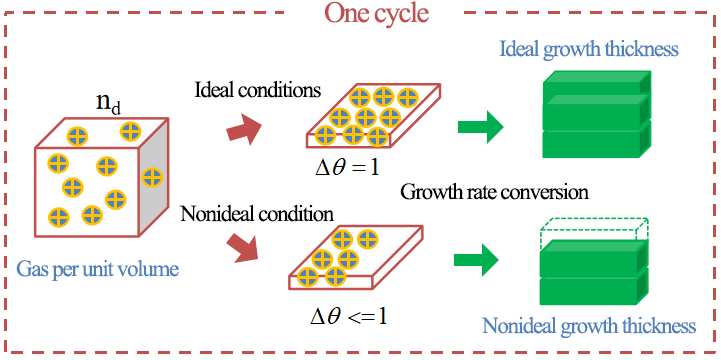
The film forming process of atomic layer deposition has excellent shape-preserving properties, but under the limit conditions, the deposition rate at the bottom of the hole will slow down, forming "poor deposition" that will affect the subsequent process steps. This model is used to simulate different substrate sizes and different reaction environments of pore structure and analyze the results, which provides help for parameter adjustment in practical application.
4.2.1. Effects of Radius and Aspect Ratio on Growth Rate
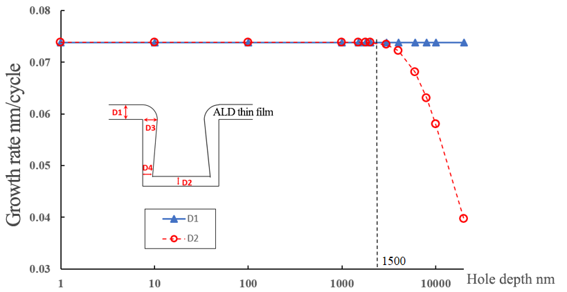
Condition 1: the basic conditions remain unchanged, the gas inlet time is 0.6s, the hole with a radius of 20nm, and the depth increases successively. After simulation, the initial growth rates of orifice and pore bottom were calculated (D1 and D3, D2 and D4 were set as equal values by the model), and the relationship between different initial depths of pores and initial growth rates was obtained, as shown in Figure 7.


Figure 7.   The growth rate at the top and bottom of the hole varies in terms of the initial conditions of the hole depth. The blue curve D1 is the initial growth rate at the top of the hole, and the red curve D2 is the initial growth rate at the bottom.
Analyze: according to the simulation results, when the hole radius is unchanged and the depth reaches a certain limit (depth-width ratio AR≈37.5), the initial growth rate begins to decline; Further discussion shows that the larger the orifice radius is, the deeper the phenomenon begins.
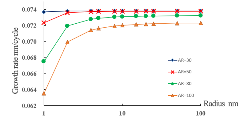
Condition 2: the ratio of depth to width (AR) is 30, 50, 80 and 100, and the radius of orifice is proportional to the depth of hole. The trend of the initial growth rate at the bottom of the hole (D2) was calculated after simulation, as shown in Figure 8.


Figure 8.   The trend of the initial growth rate at the bottom of the hole in terms of the radius of the hole with different aspect ratio.
Analyze: according to the simulation results, when the depth-width ratio of the hole is greater than 30 and remains unchanged, the initial growth rate at the bottom of the hole has an obvious downward trend with the equal proportion of radius and depth decreasing, while when the radius and depth are larger, the growth rate tends to be stable. When the depth-width ratio of the hole is less than 30 and remains unchanged, the initial growth rate at the bottom of the hole has little relationship with the radius and depth size and all remain close to the plane growth rate.
4.2.2. Combined Effects of Pressure and Inlet Time on Growth Rate
The product of pressure and entry time is defined as dose δ, where δ =P·T[12]. If the ALD film has high homogeneity in the pass structure, the input dose shall not be less than the total dose that can fill the reaction site value on the side wall surface of the pore and the reaction site value on the bottom surface. Because the actual process pressure is determined by the atomic layer deposition instrument power and cannot be changed at will, this paper only simulates different entry times.
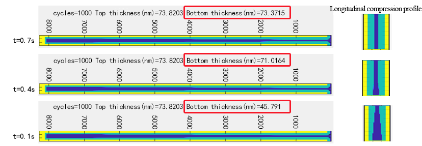
Condition: vertical pore with depth of 8000nm and radius of 100nm (AR=40), the entry time t was set at 0.7s, 0.4s and 0.1s, respectively, and 800 cycles were deposited. The simulation results are shown in Figure 9.


Figure 9.   The influence of different process time on the sedimentary profile of lateral wall of pore.
Analyze: when the pressure is constant, the entry time has a great influence on the sedimentary profile of the lateral wall. The less the entry time is, the smaller the dose can cover the inner surface of the hole. Therefore, the deeper the film goes into the bottom, the less the film thickness will be and the worse the uniformity will be. In the end, "poor deposition" will be formed, affecting the overall shape preservation.
4.2.3. Effects of Sidewall Inclination Angle on Growth Parameters
Since the algorithm of pore with dip angle adopts the CF parameter correction scheme, this paper only conducts simulation research on CF parameters with different dip angles of the pore.
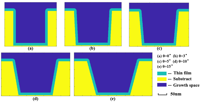
Condition: the hole bottom radius=100nm and depth L=200nm remain unchanged, the dip Angle is 0°, 3°, 5°, 10° and 15°, and the deposition cycles are 200. After the simulation, the background CF parameters are extracted, and the corresponding relationship between CF and parameters is analyzed, as shown in Figure 10, and the simulation results are shown in Figure 11.


Figure 10.   The flux distribution variation in terms of depth in pore structure with different dip Angle


Figure 11.   Profile simulation results of pore structure with different inclination angle while the hole bottom size remains unchanged.
Analyze: according to the simulation results. Even if the CF parameter is less than 1, the thin film can still be uniformly deposited. The real reason for affecting the growth rate is the ratio of the product of the flux J and the entry time t in Equation (4) to the maximum reaction site [S], which is related to the saturation entry time. With the same size at the bottom of the hole, the flux distribution at the bottom of the hole will increase with the increase of the dip angle. The reason may be that the greater the side dip Angle is, the more likely the by-products of deposition reaction will be discharged, resulting in the increase of the flux concentration that can enter the bottom of the hole, which is consistent with the actual situation.
4.2.4.   SAXP Process Profile Simulation
SAXP is an important process step of graphics transfer technology, which can be divided into SADP (self-aligned double patterning), SAQP (self-aligned quadruple patterning), etc[15,16]. This model can simulate ALD deposition steps according to SADP principle.
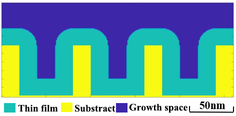
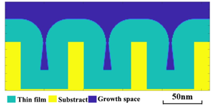
In principle, the size of the side wall as the axis should be equal to 1/3 of the radius of the hole. In this way, after subsequent etching and other processes, the figure of equal width (wall: hole =1:1) can be obtained. Therefore, the simulation conditions were set as hole radius R=60nm and depth L=60nm. The axial width is 20nm; The number of cycles is 270 (the expected growth thickness is 20nm), and the simulation results are shown in Figure 12.


Figure 12.   
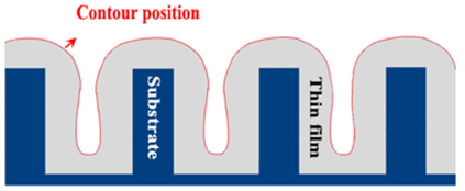
Profile simulation of the atomic layer deposition step in SADP technology.
The simulation result of film thickness is about 19.85nm, which has little error with the actual. In order to study the thin film morphology under the limit conditions, the manufacturer has actually verified the deposition contour when the cycle times are so large that the pores are almost completely covered. In this paper, the deposition contour drawing is given as shown in Figure 13(a). This model simulates the above limit conditions, and the number of cycles is changed to 390 after calculation. The simulation results are shown in Figure 13 (b).

(a)


(b)

Figure 13.   (a) Contour drawing of the actual process under the limit condition of SADP technology cycle. (b) Profile simulation result.
The simulation results are satisfactory. Except for the imprecise shape of the bottom edge of the hole, the other contour lines are consistent with the experiment, which verifies the model accuracy again.
5.   Conclusion
In this paper, a modularized ALD deposition profile prediction model based on steady state theory is proposed. The simulation results are verified to be reliable, proving that this model can achieve precise contour prediction. Through the simulation, a few key phenomenon are captured and reproduced: during the HfO2 film ALD process, the growth rate at the bottom of deep hole with high depth-to-width ratio slows down; the growth rate at the bottom of the hole also decreases when the gas entry time is below saturation threshold, resulting in defective deposition profile; the existence of the sidewall angle can help to remove the by-products at the bottom of the hole, specifically the greater the angle, the more ideal the flux distribution at the bottom of the hole. In a sum, a high-efficiency and high-precision ALD process model was established for small area patterns, this model enables opportunities for developing more complete ALD process model suitable for industrial mass production.
[1] Deng Zhang. Process Optimization and Experimental Validation of Atomic Layer Deposition with Computational Fluid Dynamics Method[D]. HuaZhong Universit of Science & Technology.
[2] Thompson S E, Parthasarathy S, Moore's law: The Future of Si microelectronics [J]. Materials Today, 9(6):20-25(2006).
[3] Berger A, et al. Metrology characterization for self-aligned double patterning[C]. Metrology, Inspection, & Process Control for Microlithography XXII. International Society for Optics and Photonics(2008).
[4] Li Ai Dong. Atomic layer deposition technology Principles and Applications[M]. Science press(2016).
[5] Remmers E M, Travis C D, Adomaitis R A. Reaction factorization for the dynamic analysis of atomic layer deposition kinetics[J]. Chemical Engineering Science, 127:374-391.
[6] Adomaitis R A. Development of a multiscale model for an atomic layer deposition process[J]. Journal of Crystal Growth , 312(8):1449-1452(2010).
[7] Dwivedi V, Adomaitis R A. Multiscale modeling of atomic layer deposition processes[C]. American Control Conference. IEEE(2009).
[8] Adomaitis, Raymond A. A Ballistic Transport and Surface Reaction Model for Simulating Atomic Layer Deposition Processes in High‐Aspect‐Ratio Nanopores[J]. Chemical Vapor Deposition, 17(10‐12):353-365(2015).
[9] Adomaitis R. A. Ballistic transport and reaction modeling of atomic layer deposition manufacturing processes. IFAC Proceedings Volumes, 44(1), 12054–12059(2011).
[10] Johnson R W, Hultqvist A, Bent S F. A brief review of atomic layer deposition: from fundamentals to applications[J]. Materials Today, 17(5):236-246(2014).
[11] Feng Li Ping, Liu Zheng Tang. Thin film technology and application[M]. Northwestern Polytechnical University Press(2016).
[12] Gordon R G, Hausmann D, Kim E, et al. A Kinetic Model for Step Coverage by Atomic Layer Deposition in Narrow Holes or Trenches[J]. Chemical Vapor Deposition, 9(2):73-78(2003).
[13] Jiang Zhong Yong, Zheng Zhong.3-D Cellular Autmata Simulation of Thin File Growth[J]. Materials Reports, 000(002):228-231(2008).
[14] Wei Qian Wei, Liu Hong Xia, Fan Ji Fei, Ma Fei, Zhang Yan Lei. Investigation of the influence of deposition temperature on ALD deposition HfO2 high k gate material. Journal of Xidian University, 39(02):164-167(2012).
[15] Berger A, Peltinov R, Ngai C, et al. Metrology characterization for self-aligned double patterning[J]. Proc Spie, 6922, 692211:1-7(2008).
[16] Sun L, Zhang X, Levi S, et al. Line edge roughness frequency analysis for SAQP process[C]. SPIE Advanced Lithography(2016).
Article and author information
Lei Qu
Chen Li
Jiang Yan
Rui Chen
Jing Zhang
Yanrong Wang
YaYi Wei
Publication records
Published: Oct. 8, 2020 (Versions2
References
Journal of Microelectronic Manufacturing