3.1
Bandgap reference start and quick start control module
Firstly, the starting circuit with self-bias function is set up for the reference power module. The module includes a reference soft-start circuit that provides a start-up bias signal; As shown in Figure 3. When the chip is just powered on, the module starts to work and a capacitor of the reference module is charged through the signal line A to make the reference circuit work
[6]. When the reference voltage reaches a certain value (about 1V), the output signal A is turned off, thus achieve a soft start function.
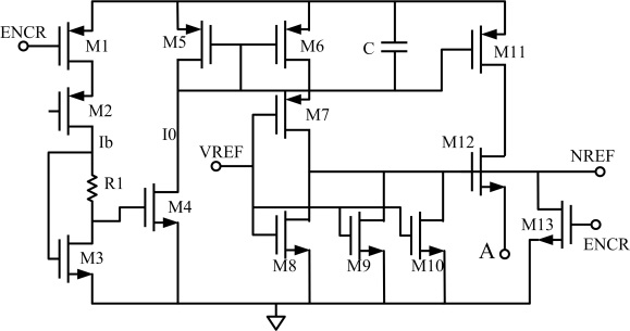
Fig3. Soft start module circuit diagram ENCR is an enable control signal that controls the generation of bias currents in this part of the circuit. The M3, M4, and R1 form a Peaking Current Mirror, and constitute a self-biasing circuit with enable control with the M1 and M2; the M7, M8, M9 and M10 form a “Not gate”, and the M11 provides startup. M12 act as a "switch," which determines whether charges capacitor. The more important part of this circuit is the determination of the charge current:
1). After the system is powered up, as long as ENCR is low, the circuit generates bias current. Since the width to length ratio of M1 is large and M2 is a reverse tube, M1 operates in the linear region and M2 operates in the saturation region, so the current can be determined by M2 and the input voltage.
2). The principle of the peak current mirror is that the resistor R1 makes M4 work in the subthreshold region.
The bias current formula is:

(1)
According to the principle of MOS peak current mirror, it can be introduced:

(2)
3.2
Quick start control module
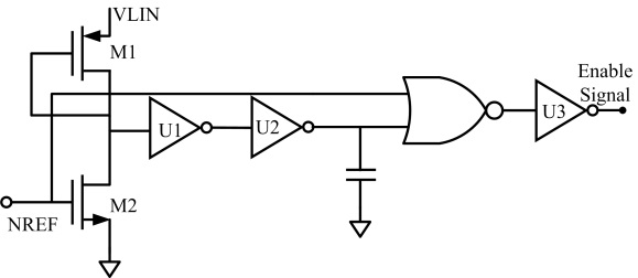
The fast charge control delays the input signal NREF to generate a fast start circuit control signal to prevent the starting circuit from generating excessive current to charge the CBYPASS. As shown in Figure 4. The bandgap circuit of the reference supply module generates an overcharge when the reference source is established. During this period, the circuit will generate a negative pulse to allow the fast-start circuit to wait for the bandgap output to stabilize slightly before charging the bypass capacitor to prevent the BYPASS terminal from overcharging when it is just charging. This circuit is a monostable flip-flop that delays the input signal.
Fig 4.Quick start circuit control circuit schematic
M1 and M2 form an active load inverter. Its output is reshaped by a two-stage inverter. The initial value of NREF is high level. After an OR gate, the initial value of the output signal is also high. With the start of the bandgap reference circuit, NREF changes from high level to low level. The output of inverter U2 must charge the capacitor and raise the potential. At this time, the output signal has changed from high level to low level. Low level is a temporary steady state; when the capacitor voltage is charged to a high level, the output signal changes from low level to high level. Therefore, the charging time of the capacitor is the output signal is low time, is the output pulse width, is the delay time of the above-mentioned fast start circuit starting operation.
When U2's input is high, the discharge current of the output capacitor is approximately:

(3)
Discharge time is:

(4)
When the input is low, the charging current of the output capacitor is approximately:

(5)
Charging time is:

(6)
It can be seen that the charging time is much longer than the discharging time, so that the output signal quickly responds to the NREF low level and guarantees sufficient low-level delay.
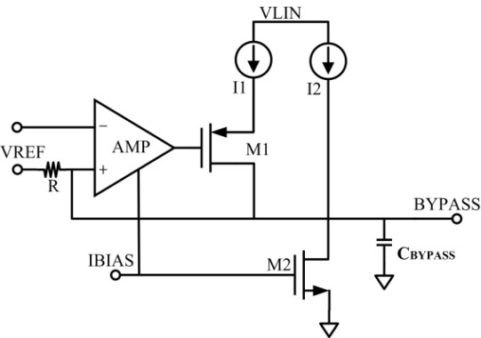
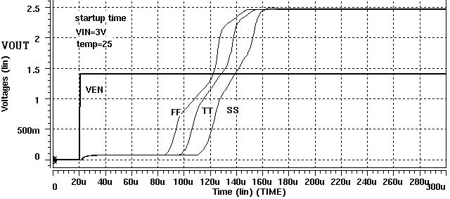
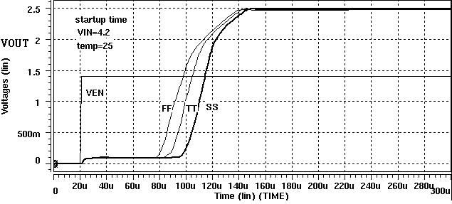
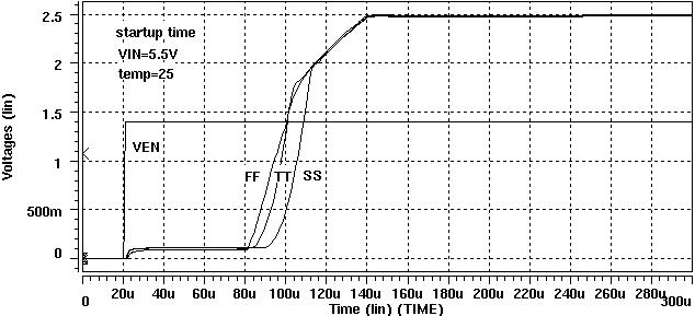
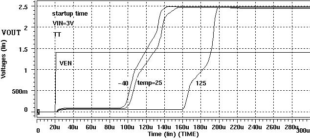
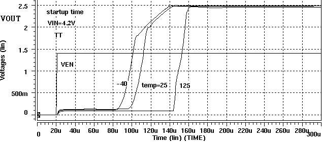
This module enables fast startup of low noise and high PSRR voltage references. When the capacitor is connected to the BYPASS pin, the output noise of the reference voltage signal will be reduced. Upon power-up, the 70uA current source inside this circuit will quickly charge the Bypass capacitor. When the reference voltage reaches 95% of its final value, the internal current source turns off and the reference gradually reaches a stable value. This speeds up the startup process. The equivalent schematic is shown in Figure 5.
Fig 5.Quick start circuit diagram The noise and ripple of the LDO regulator are primarily dependent on the characteristics of the reference. The smaller the reference voltage change, the better the regulator's output performance. To achieve low noise and high PSRR, an RC filter circuit can be used to filter out noise and increase PSRR. The principle is: the RC filter circuit generates a pole, as long as the appropriate capacitor (10nF) is selected, the pole can be moved to the low frequency to effectively filter out the noise; on the other hand, the RC filter generates the voltage from the power supply to the reference output. This pole between the two, for PSRR, is equivalent to the introduction of a zero at the same frequency, which improves the PSRR reduction at high frequencies.
However, the output impedance of a typical bandgap reference circuit is very high, and the large resistor R isolates the capacitor C. Thus, the current that VREF charges capacitor C is small, and the voltage on the BYPASS capacitor reaches a steady state reference value for a long time, thereby stabilizing The compressor output starts slowly. Therefore, a fast start circuit is added to the circuit design. When the circuit is started, the capacitor is charged with a large current, so that the reference is quickly established.
The principle of quick start is:
a. When the system is powered up, the reference source is quickly started and stable (about 30μs), and the initial voltage on the capacitor Cbypass is 0. After the reference source voltage is compared by the comparator, the output is low level, M1 is saturated, and the current source I1 is supplied to the capacitor constant current charging, BYPASS voltage rises rapidly.
b. When the BYPASS voltage rises to a certain value, the comparator outputs a high level, M1 is turned off, and I1 stops charging the capacitor.
c. Then continue to charge the capacitor by passing through the R microcurrent until the BYPASS voltage is equal to VREF.
The actual circuit is shown in Figure 6.
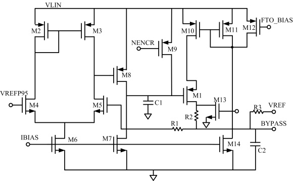
Fig 6.Quick start schematic diagram The Rail-to-Rail operational amplifier is used as a comparator to control the state of the switch M1. M10 and M11 form a current source, and the current is controlled by M14. M9 and M13 implement the enable control function. In order to prevent the quick start circuit from malfunctioning when the reference source is just started and not stable, the control module sets the FTO_BIAS signal, which is applied to the gate of M12 to control the working state of the fast start circuit. When the level is low, the circuit does not work. This module does not work if the BYPASS pin is not connected to a capacitor.The establishment and stabilization of the bandgap reference voltage takes a certain amount of time. When the first rise occurs, the IBIAS current is unstable and the circuit does not have a suitable operating point. At this time, FTO_BIAS is low level, M12 is turned on, so that M10 and M11 are turned off, and the capacitor is not charged; when the bandgap voltage VREF is substantially stabilized, FTO_BIAS is high level, and the charging control is invalid. At this time, when VBYPASS < VREFP95(95% of VREF), M1 is saturated and the bias current I1 charges the capacitor; when VBYPASS=VREFP95, M1 is turned off to stop charging the capacitor; then the small current flowing through R3 continues to charge the capacitor until VBYPASS= VREF.
The formula for charging time:

(7)