Research Article Archive Versions 2 Vol 1 (1) : 18010103 2018
Download
A Novel High Volume Manufacturing Method for Defect-free and High-yield SiN Micro-sieve Membranes
: 2018 - 08 - 22
: 2018 - 09 - 30
2325 28 0
Abstract & Keywords
Abstract: Micro-sieves have been widely used in medical treatment, quarantine, environment, agriculture, pharmacy and food processing. However, the manufacturing and yield improvement have been difficult due to multiple challenges, such as the sieve unit release defect, cracking, and KOH corrosion. In this paper, we report process details and discuss technical difficulties which are usually the root-causes for process failures, and demonstrate a reliable and high yield production of SiNx micro-sieves processed with our novel method, which is also compatible with high volume manufacturing.
Keywords: micro-sieves; high volume manufacturing; defect free; high yield
1.   Introduction
Micro-sieves have been widely used in medical treatment, quarantine, environment, agriculture, pharmacy and food processing. The fabrication of micro-sieves with different materials and aperture sizes has been reported by many groups[1] ,[2],[3],[4],[5],[6],[7],[8],[9],[10]. In this paper, we report the fabrication of SiNx micro-sieve membranes. This micro-sieve will be implemented in a bacterial detection instrument. The working principle of the product is as following: an aqueous sample solution containing bacteria flows through the micro-sieve. Bacteria, which is larger than the pore size, is screened out. The micro-sieve along with the bacteria will be sent out for imaging or component analysis.
Bacteria has three basic forms: spherical, rod and spiral. The diameter of a cocci is around 0.5 ~ 1 µm. A typical rod-shaped Escherichia coli has an average length of about 2 µm and width of about 0.5 µm. Therefore, the pore size of the micro-sieves must be smaller than 0.5 µm in order to effectively screen out a bacteria.
In our experiment, the pore size is designed as 0.45 um and silicon nitride (SiNx) is selected as the building material. SiNx has very stable mechanical and chemical properties [11] ,[12],[13],[14],[15]therefore it can hardly be eroded by water, acid or alkali. In addition to that it has high temperature stability. Most importantly, SiNx is fully compatible with the high volume semiconductor manufacturing process.
Although many research works have been accomplished in this area, very few process details are reported, especially on how to practically handle such thin and fragile porous membrane. In this paper, we report process details and discuss technical difficulties that are usually the root-causes for process failures. A reliable and high yield production of SiNx micro-sieves can be achieved with our process in a 4” semiconductor Fab.
The micro-sieve consists of two parts: a perforated SiNx film as the filter layer, and the underneath wafer supporting structure. As shown in Figure 1, the product has 17 sieve-bar units in the SiNx membrane layer, and underneath there are 17 corresponding empty bar chambers in the silicon wafer that are aligned to the sieve-bar units in the upper layer. Each sieve-bar unit is designed to be 3 mm long and 100 µm wide with an interval of 76 µm in between. Silicon micromachining allows for the fabrication of micro-sieves with well-defined pores of arbitrary size and distribution. Figure 1 shows an example of a sieve with 0.5 µm pore diameter. This design is an optimized result by considering the filtration efficiency and mechanical strength for self-supporting, since the porous SiNx membrane is suspended above the Si substrate and it must be able to withstand the fluid pressure.
2.   Fabrication
2.1.   Wafer Preparation
All experiments were conducted on 100-mm double sided polished single crystal silicon substrates (p-type, (110), 5 – 12 Ω·cm, thickness:450 µm) and there was no requirement on the resistivity or the doping type. The wafer was first cleaned with SPM liquid (SC-3) (H2SO4: H2O2: H2O) and then cleaned with APM liquid (SC-1) (NH4OH: H2O2: H2O). The proportion of liquid, cleaning time and temperature were in accordance with the international standard of semiconductor. Figure 2 shows a schematic illustration of the process for fabricating nano-sieve structures. A thin 0.6 um low-stress silicon-rich silicon nitride (Si3N4) layer was deposited over the bulk silicon substrate by low-pressure chemical-vapor deposition (LPCVD) at 770 °C, at which the temperature setting ensures a lower film stress, as shown in Figure 2 (a).


Figure 1.   The design of the micro-sieve: (a). front-side, the upper layer of the product has 17 bar sieve units, (b). back-side, 17 empty bar chambers in the silicon wafer that are aligned to the upper sieve units by front-to-back alignment, (c). top view of the micro-sieve from the front-side (17 strip sieve is the hole array), (d). stereo image of selected region in the (c) graph, with setting Rotate angle pitch (deg) -123, Yaw (dew) 240, (e). stereo image of selected region in the (c) graph, with setting Rotate angle pitch(deg) -119, Yaw(dew) 295, (f). Hole arrays of a thin microsieve with 0.45 µm pore diameter, with setting Rotate angle pitch (deg) -15, Yaw (dew) 0.
A photosensitive layer of SPR 955-CM was spin-coated (30s at 4000 rpm,) on the underlying nitride layer by SVG11 with a post-applied baking temperature of 90 °C for 90 seconds. The resist was then exposed by ASML PAS5000 stepper. After the exposure, post-exposure baking (PEB) of 120 °C for 90s was performed. Following that the wafers were developed for 60s and then rinsed with deionized (DI) water. As a result, the resist layer contained high density holes that were parallel each other and the hole apertures were the same, as shown in Figure 2 (b). After photolithography the wafers were etched, a reactive ion etch (RIE) process was used to transfer exposed resist patterns into the underlying nitride layer by Lam Rainbow 4520 by using CHF3/CF4 plasma chemistries. The exposed nitride layer region where the resist was removed goes through anisotropic etching process with the silicon substrate as an etch stop, as shown in Figure 2 (c). In Figure 2 (d), by employing the Tempress system, a high stress silicon nitride film with a thickness of 200 Å was formed to top of the wafer and the open areas in the patterned Si3N4 layer were covered. For the sake of convenience, we name it the second layer of silicon nitride (2nd nitride layer), in which the diameter of the holes was decreased, and the corrosion of the wafer front will be prohibited in the last step as shown in Figure 2 (g). In Figure 2 (e), a photo-resist layer was formed on the nitride layer at the wafer backside. Using photolithography with EVG620 which is featured with the bottom side alignment system, the photo resist layer pattern was defined into a reverse hard mask aligned to the holes array on the wafer front side. Using an RIE process, the wafer backside window will be opened in the nitride layer, as Figure 2 (f). Finally, wet anisotropic etching started from the backside of the wafer until the perforated Si3N4 layer released by KOH (33%, 80℃), while high pressure nitride in the openings acted as plug at the wafer front side, which will auto break when hang in the air as its high press, as Figure 2 (g).


Figure 2.   Schematic diagram of the process flow for fabricating nano-sieve structures: (a) Si3N4 deposition by LPCVD, (b) photolithography of the sieve unit pattern (c) the sieve unit is produced after RIE, (d) 2nd nitride layer deposition by the Tempress system, (e) backside photolithography by EVG620, (f) backside window open by RIE, (g) wet etching from wafer backside.
To separate the single sieve device from the wafer after the process is completed, we used a conventional wafer laser scribing process. Firstly, the operator took out a piece of wafer and place it facing down on the working panel of the surface mounting machine, and then put on the wafer frame. Secondly, the operator pulled out the Ultraviolet Rays (UV) tape and attached it to both front and rear parts of the mounter machine, then scraped off the tape with a hob and teared off. Of course, you need to check whether there was a bubble between the UV tape and the wafer. Usually, a bubble larger than 0.5mm was not allowed. The next step was the wafer segmentation using laser. The final step, the wafer was then placed in a die expansion tool that stretches the tape to introduce space in between the dice. Typically, die expansion tool uses a movable anvil that pushes axially on the wafer to expand the tape to introduce space in between the dice.
2.2.   Issus in Fabrication
The results achieved in our pi-run lot were bad with very low product yield. We identified three major issues through investigation: the substantial part of the sieving membrane was not completely released; the released sieve unit cracked or tore so badly that one can’t even find one perfect cell among hundreds with optical microscopy; after KOH corrosion step, there might be destructive mechanical damage to this product during dicing process. The details are as followings:
2.2.1.   Effective Release of Sieve Units
2.2.1.   1. Issue
As shown in Figure 3 (a), substantial part of the sieving membrane was not fully released while the top sieving structure and bottom window have the same length, which meant that not all perforated silicon nitride membranes were released from the silicon substrate.
2.2.1.   2. Analysis
It was found that the etch resistance of Si has anisotropic properties. In our experiments, it was also confirmed that the shape of a KOH etched trench in (110) wafers was radically different, as shown in Figure 3 (a). A groove etched in (110) wafers has the appearance of a complex polygon delineated by six {111} planes, four vertical and two slanted, which disturb the possibility to make small channels, as shown in Figure 3 (b). As a result, patterns in the shade of oblique planes on the front side can’t release if etch the silicon only from the backside. The four vertical {111} planes intersect to form a parallelogram with an inside angle of 70.5°. Due to anisotropic etching in {110}-oriented silicon, the length design of top sieving structure and bottom window should involve some compensation.


Figure 3.   (a) Substantial part of the sieving membrane was not fully released, (b) illustration of the anisotropic etching in {110}-oriented silicon. Etched structures are delineated by four vertical {111} planes and two slanted {111} planes. The vertical {111} planes intersect at an angle of 70.5° [18], (c) optical microscopy images of the final product results after KOH etching.


Figure 4.   Optical microscopy images show that SiN film broke in KOH solution without protection.
2.2.1.   3. Solution and Results
Instead of the conventional compensation angle method, the approach we used was correcting backside mask design. As a result, etching one rectangle with the length of 3500 um, width of 100 um and depth into the Si wafer of 500 um created a suspended area covering the sieving structure that measures around 3000 um by 100 um, as shown in Figure 3 (c).
2.2.2.   Membrane Release
2.2.2.   1. Analysis: Wet Etching through the Pores
In 1998, S. Kuiper introduced the discovery that for pores smaller than 1 um, the pressure build-up due to hydrogen gas formation can be large enough to cause rupture of the membrane during the positive structure release by KOH etching [12] ,[13]. However, till now there are no reports that can describe the exact mechanism behind this phenomenon.
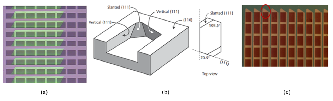
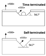
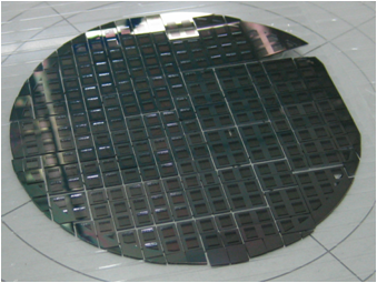
In order to explore the intrinsic mechanism, we have been doing a considerable amount of experimental works. For 500 um thick wafers it’s impossible to finish corrosion in short times, however we found rupture of the sieve units, with (100) wafer, shown as Figure 4. It is highly likely that the rupture happens during the wet etching though the pores.
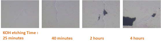
There is one hypothesis assuming that it’s hydrogen bubbles rupturing the upper layer, however we see little support to this assumption. With 0.45 um diameter cylindrical holes in LPCVD silicon nitride layer as hard mask at the front side, the KOH Etching of (100) Si will be self-terminated in several minutes, therefore it’s so questionable that how the hydrogen bubbles could create cracks to the filtration structure if hydrogen bubble just adsorbs the wet etching surface, as shown in Figure 5.


Figure 5.   KOH Etching of (100) Si wafer.
A variety of theories have been formulated to explain the irradiation damage due to implanted ions in metals which is mainly related to the nuclear reactor technology. So far, an especially elegant procedure has been suggested by Bruel and termed Smart-Cut. It is based on the hydrogen implantation before bonding which leads to the splitting of silicon wafers along hydrogen-filled micro-cracks, and the cracks are induced by the precipitation of the implanted hydrogen during a heating step after bonding. When temperature changes, material mismatch may cause defect growth such as cavities which generate lot of stresses at the interface. It is also the only mechanism by which the thermal mismatch plays a role in wafer splitting in the Smart-Cut process. As the KOH etching is an exothermic process, the hydrogen is not gathering on the wet etching surface but rather diffuses along the interface between Si and LPSiN layer [24].
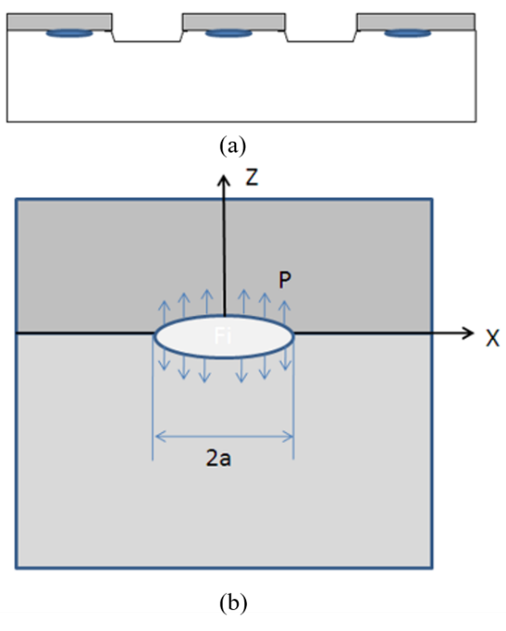
As showed in Figure 6, with a uniform pressure loading over the entire bubble surface inside, the stress will induce cleavage at the interface. As the sieving layer contains a periodic array of holes, hydrogen bubbles are distributed in the interface of Si and LPSiN layer. As hydrogen molecules are gathering, cracks in the filtration membrane will occur when the shear force per unit rises to the maximum stress that the LPSiN film can withstand.


Figure 6.   Crack model of a periodic array with hydrogen bubble distributed in the interface of Si and LPSiN layer, (b) the crack configuration of the fracture mechanics model.
2.2.2.2. Special Care to Protect the Front Side against KOH Solution
Although the theory remains to be studied, we try to solve the problem. SF6/O2 plasma dry etching from the front side of the wafer through the pores was employed [12] ,[13]. However, SF6/O2 plasma does not perform enough lateral etch (undercut) of the silicon to connect the trenches. And the silicon nitride exhibits a poor etch resistance to the plasma and as a result at room temperature the membrane shows a significant under-etch. As the apparatus is a single wafer etcher and the whole process takes about one hour, this method is super time-consuming.
An idea to ensure a reasonable fabrication yield was employed, in which special care was taken to protect the front side against the KOH solution [14]. Black wax and polymer coat were implemented as a protective coating for KOH etching. However, after dissolution of wax in toluene solvent there is still residual of black wax, which is not acceptable for operating products. By using a polymer coat to mount the sample to a glass and black wax to seal the sample and the glass, we only obtained a fabrication yield of 31%. Actually we tried AR-PC 504 on sieving layer side of wafers against wet etching processes, but failed as the resist layer peels off in lessthan one hours from the substrate in 33% KOH solution and at 80℃ temperature. Therefore it would be worthy trying to attack the wet etching problems from a different perspective.
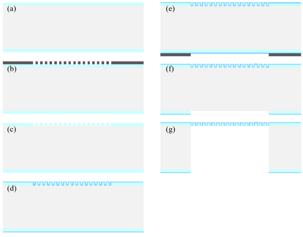
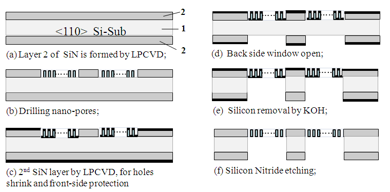
Fortunately, we eventually achieved a reliable front side protection against KOH etching through the pores. We improved the frication process shown in Figure 2 by depositing a 2nd 200 Å thick thin layer of high stress SiN by LPCVD to both sides, which will effectively prevent the front side from KOH etching in case of hydrogen gas induced rupture build-up during wet etching, as shown in Figure 7. The 200 Å thick SiN at the bottom of the holes will automatically break easily and fall off when the silicon beneath is etched by KOH. As a result we achieved much improved yield results.


Figure 7.   Improved fabrication process with special care of front side against KOH etching.
2.2.2.   3. Results
With SiNx film’s special care against KOH erosion, only 3 chips were found to have cracks among 108 individual micro-sieves that were randomly selected. As a result, the yield greatly increased comparing to that of the black wax or alkali resistant resist before.
2.2.3.   Dicing
2.2.3.   1. Issue
In the manufacturing of integrated circuits, wafer dicing is the process that separates the die from a wafer after the wafer process is accomplished. The dicing process includes mechanical or laser dicing. Due to the brittleness of silicon materials, especially the free standing structure membrane such as suspended SiNx film in this product, both the traditional dicing saw and the most advanced stealth laser scribing (Stealth Dicing, SD) technology produce mechanical stress on the front and back of the wafer, inducing the reduction of mechanical strength and even the emergence of fracture fragments, etc. However, even a small crack will render the micro sieve unsuited for its purpose of catching microorganisms, because microorganisms will pass the membrane through the crack(s) without being detected. In order to address this issue, we managed to worked with the dicing process engineer and found a suitable dicing process for the product.
2.2.3.   2. Root Cause
Wafer mount is the wafer fixing process before cutting, in which a blue UV film is attached to the front side of the wafer and fixed on a metal frame. The UV film can be firmly adhered to the wafer so that even after dicing the die will not be scattered. Of course, all different methods require firstly protecting the wafer so that its components face down and attach to the UV film to allow the cutting from the back of the wafer. The next step is the laser dicing followed by wafer expanding. The wafer expansion machine is used to expand the bonded UV film, and then the spacer between closely spaced chips is stretched so that you can take down one after another for packaging, as shown in Figure 8. You can take out and remount wafers to start over the process.


Figure 8.   After wafer expansion, the closely spaced chip spacing is stretched.
2.2.3.   3. Solution
We created a novel double foil method by using a double UV membrane to attach to the frame and partially remove material in the first UV layer according to the layout of the chip, which is equivalent to elastically inserting a blank space, in order to avoid the situation that the fragile part of chip component touches the UV tape. The method includes the following steps:
Firstly, the frame is attached with two layers of UV film. Considering the follow-up process, we should choose different colors for the two layers of UV film and make the first layer as thick as possible. In this product we selected blue and green colors for the first and second UV film respectively, with type of glue: 0636-00.
The second step is cutting the first layer of UV film according to the chip layout, it’s worth noting that the cutting depth of the tool must be controlled in order not to affect the second UV layer. And the cutting area must be corresponding to the part of the chip’s fragile unit. After that we remove the cutting area carefully using tweezers, and the bi-layer UV film on the frame presents a three-dimensional structure as shown in Figure 9.


Figure 9.   After remove the cutting area on 1st UV layer, (a) the bi-layer UV film on the Frame presents a three-dimensional structure, (b) cross section along the red line in (a).
The third step is the wafer mounting onto the 3D film structure prepared in the previous step, with alignment to affix chip periphery with scribe line to the reserved on the first UV membrane, as shown in Figure 10. In other words, the chip fragile area lies out in the first UV layer’s hollowed space without contact with UV film.


Figure 10.   Wafer alignment mounting, (a) chip periphery with scribe line to the reserved on the first UV membrane, (b) cross section along the red line in (a).
The following step is the laser scribing, using the most advanced SD technology with the wafer dicing machines: ML200 of accretech.
The final step is the wafer expansion, in which the wafers are mounted on UV film for electronic packaging and product assembly. During the wafer expansion the tension of the UV film will pull the cut dice apart, the pulling force plays a role in wafer cutting section, for instance, the portion of the contact between the wafer and the first layer of the UV film as shown in Figure 10(b). Therefore, as chip’s mechanical fragile parts lie in hollowed out space there is no contact with the UV film, which successfully avoiding the tensile impact of UV film.
2.2.3.   4. Results
Optical microscopy inspection showed that no fragmentation of debris was found on the UV film, and the samples were accepted for stress testing.
3.   Performance Test Results
3.1.   Integrity
Because of the special purpose, this product must not contain hair cracks or pinholes. Therefore filtration tests were performed on reference samples to identify the filtration quality.
With SiNx film’s special care against KOH erosion, among 108 individual micro-sieves random selected there were only 3 chips found cracks. The yield was greatly increased comparing to that of the black wax or alkali resistant resist before.
3.2.   Strength
Micro-sieves must remain intact during filtration of liquids through centrifuge or vacuum filtrations. During these processes, mechanical load equals 1 to 3 bar pressure differences. A non-destructive testing method of the micro-sieve strength has been developed by applying air pressure on the micro-sieves. Test levels up to 6 bar air pressure. A custom tool has been developed to maintain the air pressure during this test.
In total 15 micro-sieves have been tested to obtain a set of ten for filtration purposes. Acceptance value was set to 4 bar for numbers 9 ‒ 15. For the functional filtration test at 1 bar, the yield acceptance value is 65% for CCM strength test.
3.3.   Filtration
The above set of micro-sieves then was used for filtration tests. Unfortunately, the results of the filtration tests could not be analyzed with MuScan due to assembly issues that were caused by burrs during laser dicing.
3.4.   Cleanliness
Micro-sieves are not allowed to contain imperfections like dust particles or (hair) cracks. Microscopic imaging can provide additional information on the conditions of the micro-sieve. In general, the quality of this product meets the criteria.
Table 1.   15 micro-sieves that have been tested.


Figure 11.   Product design.
4.   Conclusion
As shown in Figure 11, the plane size is 5mm by 5 mm, a silicon nitride layer is plated on the silicon wafer with 17 bars of sieve unit that is featured with 100 um width and 76 um interval, and is perforated with pore diameter of 0.45 um. It’s noteworthy that since the process capacity can reach 100 nm limit with the 248 nm KrF lithography equipment, we can make any design & any pore size according to the practical needs.
The wafers were diced, and chips were shipped to third party for filtration and pressure tests. Comparing to black wax and alkali resistant resist with unstable etching performance in alkaline environment (33% KOH, 80℃), the KOH protective technique presented in this study shows good performance for the safer release in KOH of suspended sieving membrane in a mass production process.
This novel technology may be used to boost the fabrication yield of other kinds of thin, strong and defect-free membranes. And SiN micro-sieve membranes with uniform cylindrical pores about 450 nm may be used in new applications.
For the future work, due to the crystal characteristics of (110) wafer in KOH solution, we are now exploring the wet etching dicing instead of laser for cost saving purpose, and will present the result a following report.
Acknowledgement
We are grateful to the Key Laboratory of Microelectronics Devices and Integrated Technology, Institute of Microelectronics, Chinese Academy of Sciences for financial support.
[1] C. van Rijn, "Nano and Micro Engineered Membrane Technology," (Elsevier, Amsterdam, 2004).
[2] S. Kuiper, C. van Rijn, W. Nijdam, and M. Elwenspoek, "Development and applications of very high flux microfiltration membranes," J. Membr. Sci.,150 , 1 (1998).
[3] C. van Rijn, W. Nijdam, S. Kuiper, G. J. Veldhuis, et al., "Microsieves made with laser interference lithography for micro-filtration applications," J. Micromech. Microeng.,9 , 170 (1999).
[4] R. M. de Vos, and H. Verweij, "High-flux silica membranes for gas separation," Science,279 , 1710 (1998).
[5] T. Tsuru, "Inorganic Porous Membranes for Liquid Phase Separation," Sep. Purif. Rev.,30 , 191 (2001).
[6] L. Leoni, and T. A. Desai, "Nanoporous biocapsules for the encapsulation of insulinoma cells: biotransport and biocompatibility considerations," IEEE Trans. Biomed. Eng.,48 , 1335 (2001).
[7] H. Zhu et al., "Analysis of yeast protein kinases using protein chips," Nat. Gen.,26 , 283 (2000).
[8] C. D. Lytle, L. B. Routson, N. B. Jain, M. R. Myers, et al., "Virus passage through track-etch membranes modified by salinity and a nonionic surfactant," Appl. Environ. Microbiol.,65 , 2773 (1999).
[9] C. van Rijn, W. Nijdam, and M. Elwenspoek, "A microsieve for leukocyte depletion of erythrocyte concentrates," IEEE Trans. Magn.,1 , 256 (1996).
[10] C. van Rijn, M. van der Wekken, W. Nijdam, and M. Elwenspoek, "Deflection and maximum load of microfiltration membrane sieves made with silicon micromachining," J. Microelectromech. Syst.,6 , 48 (1997).
[11] C. M. Kurz and H. Thielecke, "Characterisation of the deflection of thin perforated SiN membranes of micro-hole array chips used for the cell selection," Microelectron. Eng., 88 , 1782 (2011).
[12] J. Chen, M. A. Reed, A. M. Rawlett, and J. M. Tour, "Large on-off ratios and negative differential resistance in a molecular electronic device," Science,286 , 1550 (1999).
[13] K. M. Vaeth, "Micromachined Microsieves With High Aspect Ratio Features," J. Microelectromech. Syst.,21 , 68 (2012).
[14] S. Kuiper, C. van Rijn, W. Nijdam, and M. C. Elwenspoek, "Development and applications of very high flux microfiltration membranes," J. Membr. Sci.,150 , 1 (1998).
[15] S. Kuiper, M. J. Boer, C. van Rijn, W. Nijdam, et al., "Wet and dry etching techniques for the release of sub-micrometre perforated membranes," J. Micromech. Microeng.,10 , 171 (2000).
[16] L. F. Houlet, W. Shin, M. Nishibori, N. Izu, et al., "Safe membrane-releasing process for thermoelectric hydrogen gas sensor," SENSORS, 2007 IEEE, Atlanta, GA, 2007, pp. 1032-1035.
[17] C. van Rijn, M. van der Wekken, W. Nijdam, and M. Elwenspoek, "Deflection and maximum load of microfiltration membrane sieves made with silicon micromachining," J. Microelectromech. Syst., 6, 48 (1997).
[18] H. D. Tong, F. C. Gielens, J. G. E. Gardeniers, H. V. Jansen, et al., "Microsieve supporting palladium-silver alloy membrane and application to hydrogen separation," J. Microelectromech. Syst.,14 , 113 (2005).
[19] D. L. Kendall, "Vertical etching of silicon at very high aspect ratios," Ann. Rev. Mater. Res.,9 , 373 (1979).
[20] N. Maluf and K. Williams, "An introduction to microelectromechanical systems engineering, second edition," (Artech House, Norwood,2004).
[21] M. M. Deshmukh, D. C. Ralph, M. Thomas, and J. Silcox, "Nanofabrication using a stencil mask," Appl Phys. Lett.,75 , 1631 (1999).
[22] C. Schmidt, M. Mayer, H. Vogel, "A chip-based biosensor for the functional analysis of single ion channels," Angew. Chem.,39 , 3137 (2000).
[23] J. E. M. McGeoch, M. W. McGeoch, D. J. Carter, R.F. Schuman, et al., "Biological-to-electronic interface with pores of ATP synthase subunit C in silicon nitride barrier," Med. Bio. Eng. Comp.,38 , 113 (2000).
[24] T. Schenkel, V. Radmilovic, E. A. Stach, S. J. Park, et al., "Formation of a new nanometer wide holes in membranes with a dual beam focused ion beam system," J. Vac. Sci. Technol. B,21 , 2720 (2003).
[25] J. Li, D. Stein, C. McMullan, D. Branton, et al., "Ion-beam sculpting at nanometre length scales," Nature,412 , 166 (2001).
[26] U. Gösele, Q.-Y. Tong, A. Schumacher, G. Kräuter, et al., "Wafer bonding for microsystems technologies Sensors and Actuators," Sensor Actuat A-Phys,74 , 161 (1999).
Article and author information
Yansong Liu
Chao Zhao
Lisong Dong
Rui Chen
Yayi Wei
weiyayi@ime.ac.cn
Publication records
Published: Sept. 30, 2018 (Versions2
References
Journal of Microelectronic Manufacturing