In currently, the IC packaging manufacturers have developed FOPLP technology, including Samsung Electronics, Nepes Laweh, Innolux Display Group, Powertech Technology, ASE group, SPIL and TSMC. The projects and progress of FOPLP encapsulation mode developed by various manufacturers were listed in Table 1. The four packaging manufactures including Powertech Technology, ASE group, Innolux Display Group and SMECO have all applied FOPLP technology in PMIC packaging, and the size of packaging panel reached 515x510mm, even 600x600mm. The SPIL and TSMC mostly applied FOPLP technology in the packaging of AI CPU., and the size of packaging panel also reached 515x510mm.
Samsung Electronics was the first manufacturer of FOPLP for realizing mass production. Samsung Electronics decided to establish a special working group and compete with TSMC's InFO-WLP (Fan Out Wafer Level Packaging) technology after failing to compete with TSMC for an Apple smartphone processor order in 2015. Samsung Electronics built the team group for strategically develop FOPLP technology based on its subsidiary Samsung Electric. Samsung Electronics acquired Samsung Electric's semiconductor fanout panel level business in 2019. Samsung Electronics transferred some old LCD display production lines into packaging factories to fully committed to developing FOPLP technology packaging based on its more advanced packaging than FOWLP. Based on the advantages that FOPLP was a technology for packaging on square substrate panels rather than circular substrates such as wafers, FOPLP had a higher competitiveness in cost than other packaging technology. The production line established in Tian'an, Chungcheongnam by Samsung Electric was applied in the processor packaging of smart watch Galaxy Watch. This is the first global mass production of FOPLP. Samsung Eletric initially used 510x415mm sized panels to manufacture FOPLP, and also developed panels up to 800x600mm. Samsung Electronics adhered to use plastic substrates by emphasizing their advantages of low cost, mature technology and flexibility, which was suitable for cost sensitive applications such as storage chips.[45] In the early stages, FOPLP mass production was achieved by using plastic substrate with facing the problem of thermal warping. While, Samsung Electronics has announced the investment in the research of glass substrate in 2024 and planed to launch commercial products for meeting the demanding of high-performance computing (HPC) and AI chips in 2026.[46]
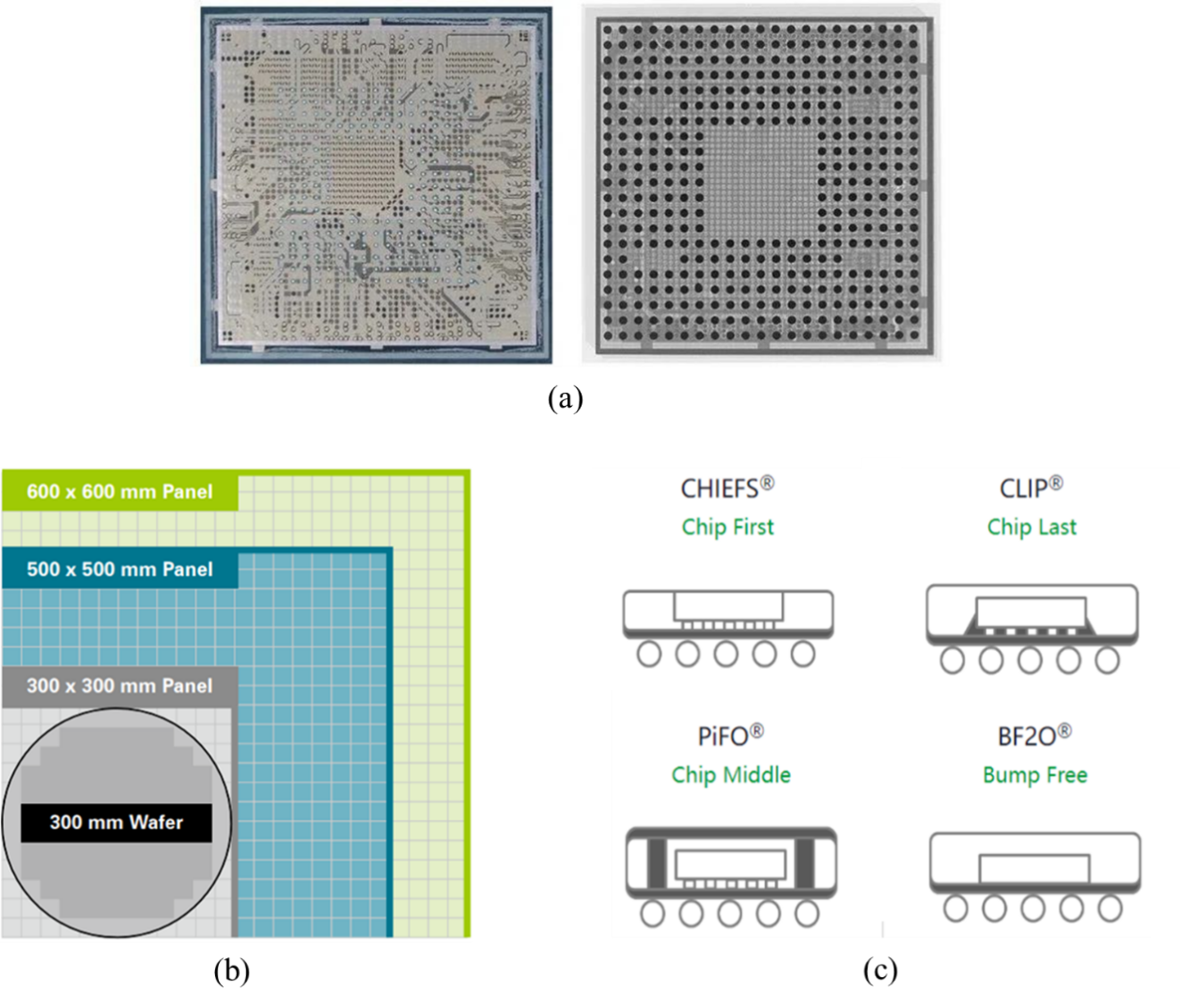
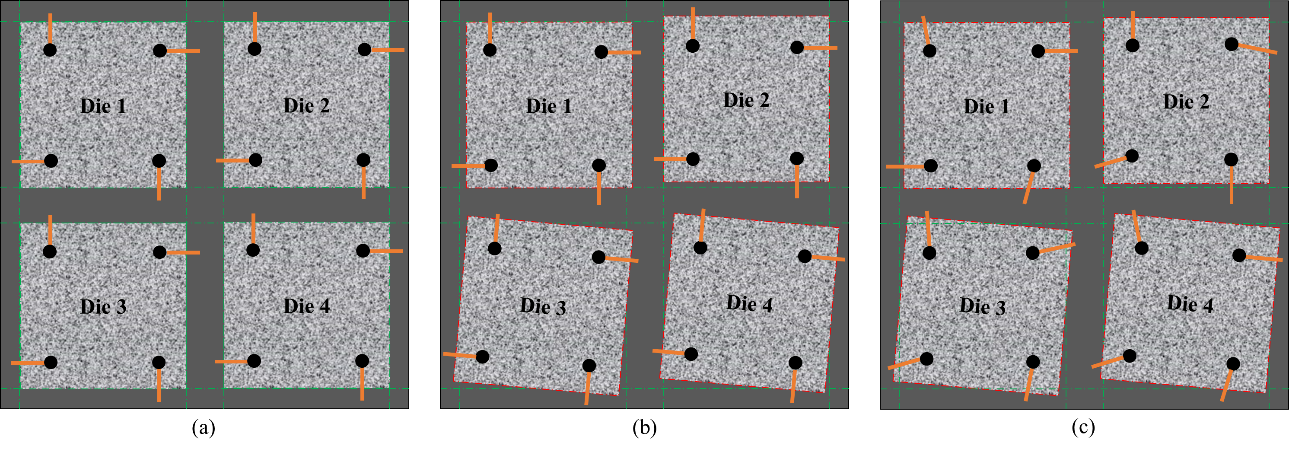
Nepes Laweh is also a leading company in the system semiconductor industry with advanced fanout packaging solutions. Nepes Laweh began to develop the FOPLP technology since 2014, when it began to get mass production of FOWLP by integrating its subsidiary's TSP (touch screen panel) equipment technology. Based on the advanced packaging technology and subsidiary display technology, Nepes Laweh had achieved fanout packaging on 600mm large square panels in 2017. Nepes Laweh also acquired a fanout factory located in the Philippines and the latest fanout technology in 2019. Nepes Laweh have launched its first FOPLP business by using 600x600mm panels, which had a fully mass production in 2021. The architecture of FOLPL devices developed by Nepes Laweh was showed in Figure 1a.
Innolux Display Group has proposed an unprecedented concept named panel semiconductor for the first time. The advanced packaging technology that can highly integrate chips has become one of the important directions for the development of mass innovation in the cross-border semiconductor industry. Innolux Display Group had activated the existing G3.5 production line, with the glass panel size of 620mmx750mm, and the line width ranging from 2um to 10um. The panel size of FOPLP technology developed by Innolux Display Group was showed in Figure 1b. The panel size of FOPLP have developed included 300mmx300mm, 500mmx500mm, 600mmx600mm and 620mmx750mm. The packaging area of the panel with size of 620mmx750mm was 7 times of the packaging area of 300mm glass wafer. With the panel warpage being overcome, the FOPLP technology could provide a more competitive costs and creating greater profit value based on the advantages of accommodating more I/O numbers, smaller size, stronger efficiency, saving power consumption and so on. In 2017, Innolux Display Group had taken the lead in transforming low generation panel factories into FOPLP production lines for accumulating experience in panel level packaging. By utilizing panel manufacturing foundation, which can optimize carrier utilization rate (>95%) and reduce production costs obviously.[47]
Powertech Technology had always held a leading position in global packaging and testing services, and was also one of the leaders in the layout and mass production of FOPLP technology. In 2018, Powertech Technology built the first mass production line with using FOPLP technology in the field of advanced packaging in 2018, the related technology applied to MediaTek PMIC and audio transceivers successfully. Powertech Technology had provided four packaging structures in FOPLP technology, including CHIEFS solution based on chip first, CLIP solution based on chip last, PiFO solution based on chip middle, and Bump FreeBF2O. The structure of FOPLP devices developed by Powertech Technology was showed as Figure 1c.
Figure 1.
The architecture of FOPLP technology: (a) the architecture of FOPLP devices developed by Nepes Laweh, (b) the panel size of FOPLP technology developed by Innolux Display Group, (c) the structure of FOPLP devices developed by Powertech Technology. ASE group is one of the earliest leading manufacturers to layout FOPLP technology. At the end of 2019, ASE had completed the construction of the production line, and the mass production was also carried out in 2020. In order to meet the integration needs of networks and artificial intelligence applications that require larger memory and computing power, ASE also launched the VIPack advanced packaging platform, for providing vertical interconnection integrated packaging solutions in 2022. VIPack is an advanced interconnect technology solution with 3D heterogeneous integration as the key technology, establishing a complete collaborative platform. ASE Group has actively invested in experimental production of FOPLP technology and plan to conduct trial production in 2025. FOPLP technology was plan to coexist and develop with chip on wafer on substrate (CoWoS) technology by covering different application scenarios (such as consumer electronics and AI servers).[48]
By placing bet on glass substrate, TSMC highlighted its high thermal stability and flatness, which can achieve tighter interconnect spacing and is suitable for high-performance chips (such as AI, HPC). With high yield and advanced OEM process, TSMC has occupied over 50% of the global OEM market share. Based on high barriers to entry of Glass substrate technology, TSMC has strengthened its leadership position in the high-end chip packaging market.[49]
Apart from those foreign manufacturers have developed FOPLP technology as mentioned above, there are also many domestic manufacturers already having mass-produced or having production capacity such as Sipan Microelectronics (Chongqing) Co., Ltd., ECHINT Technology, Guangdong Fozhixin Microelectronics, Tianxin Interconnect and so on. The Sipan Microelectronics (Chongqing) Co., Ltd. had engaged in panel level packaging business in 2018, and its FOPLP technology can effectively solve the problem of high cost of chiplet packaging and is more suitable for heterogeneous integration of power semiconductor packaging. ECHINT Technology is a leader manufacturer in the field of board level high-density packaging technology in China. This company have mainly engaged in board level system packaging and testing integrated circuit business with a board size of 510mm x 515mm. Guangdong Fozhixin Microelectronics have created an advanced circuit creation process (i-FOSATM) for semi additive fanout packaging by combining the advantages of existing semiconductor process equipment and back-end board process equipment. The i-FOSATM technology has the characteristics of advanced technology, reasonable cost, and supply chain security. It has also built the first domestic high-performance and cost-effective board level fanout packaging research line and demonstration line. Tianxin Interconnect is a wholly-owned subsidiary of Shennan Circuit and also has a Board Level FOPLP platform, which can provide customers semiconductor device module packaging solutions and semiconductor testing interface solutions with highly integrated and miniaturized.
At present, as one of the most important and rapidly developing industries, the new energy vehicles could also promote the synchronous development of FOPLP technology by benefiting from the increasing demand of domestically produced automotive grade chips coming from electric vehicles.[50] The advantages of FOPLP technology used in the field of new energy vehicles mainly include five aspects, which were listed as below. Firstly, the lower cost effectiveness. FOPLP technology has significant cost advantages compared to other packaging methods by encapsulating more chips in large panel formats. This technology can provide flexibility in handling various materials and sizes of panels, thereby improving productivity and output, while reducing ownership costs in large-scale manufacturing environments. Secondly, the more scalability and flexibility. FOPLP technology can support larger scale production and can adapt to panels of different materials and sizes, which could make the production process more flexible and able to meet the needs of different new energy vehicle manufacturers. Thirdly, the greater integration capability. FOPLP technology makes it possible for the integration of multiple chips and passive components within a single package, which is particularly important for high-power electronic devices in new energy vehicles based on the fact that it can significantly improve circuit integration and reduce overall system complexity and volume. Fourthly, the higher performance improvement. With the continuous advancement of technology, FOPLP has begun to be applied in fields such as high-performance computing and artificial intelligence, which means that battery management systems and other critical electronic devices can achieve higher performance in new energy vehicles, thus could enhance the overall performance and efficiency of the vehicle. Fifth, more mature supply chain development. With the increasing demand of FOPLP technology, the supply chain is gradually maturing. The shortage of initial equipment and materials is expected to be resolved, which will help to further reduce the production costs and improve production efficiency. In summary, FOPLP technology provides a cost-effective, flexible and high-performance packaging solution in the field of new energy vehicles, which is of great significance for promoting the development and popularization of new energy vehicle technology.[51]
In currently, universities and research institutions were mostly focus on the research of material and process optimization in the field of FOPLP technology, mainly included materials innovation, process simulation, heterogeneous integration and university-industry cooperation.[52] For the material innovation, low dielectric constant (Low-K) dielectric material and high thermal conductivity plastic encapsulation material were developed to reduce signal loss and solve heat dissipation problems, respectively. For the process simulation, panel warpage controlling was optimized by simulation techniques, such as using finite element analysis (FEA) to predict thermal stress distribution. For the heterogeneous integration, a few research was developed to explore the combination between photonic chips and FOPLP for improving the communication speed (such as silicon photonics integration). For the university-industry cooperation, a few major companies chose to collaborate with universities to new develop technologies. For example, Samsung Electronics has collaborated with universities to publish papers which was related to FOPLP technology for promoting a few technological breakthroughs in 2.5D packaging.
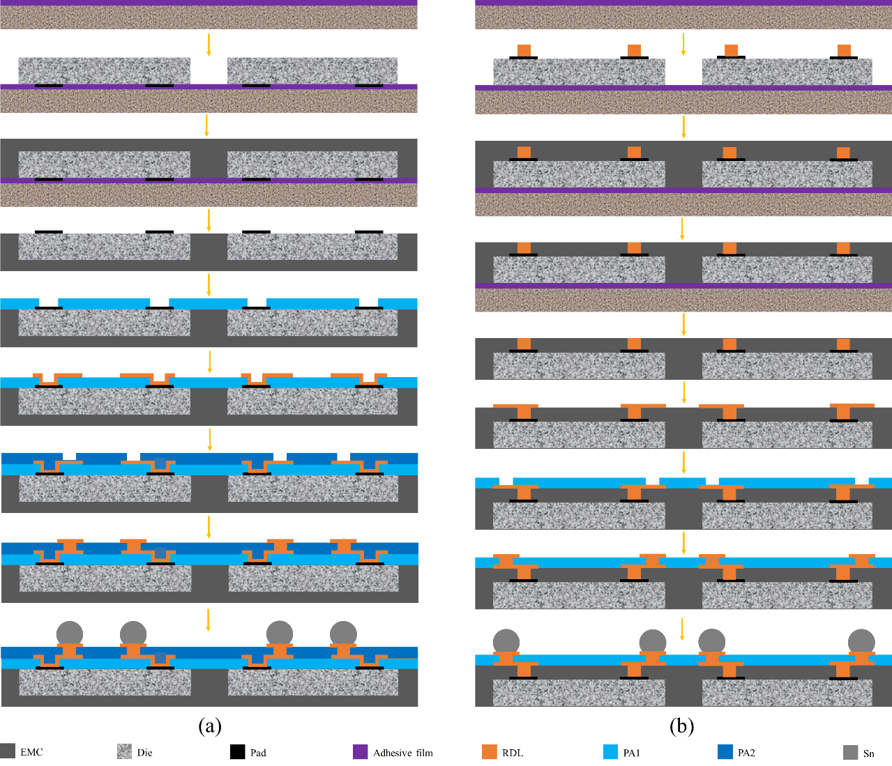
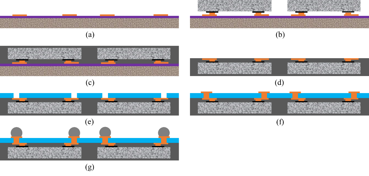
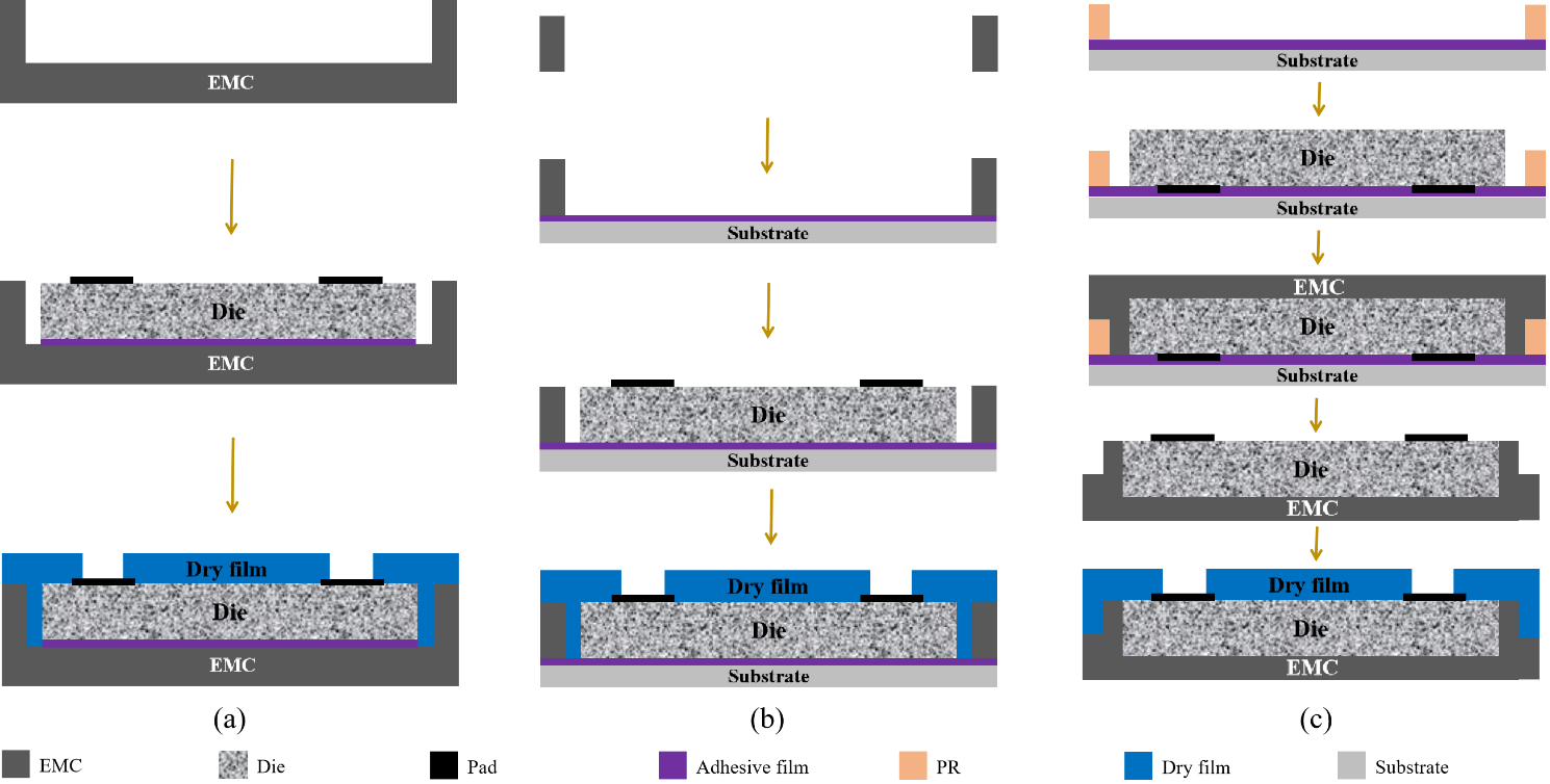
Figure 2.
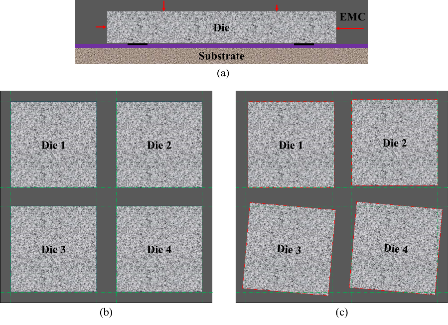
The architecture of process flow for FOPLP technology with die first: (a) based on chip face down, (b) based on chip face up. For the prediction of future technology roadmap, FOPLP technology may have great development in a few aspects, mainly including the expansion of panel size, development of 3D-FOPLP technology, material innovation used in FOPLP, automation and intelligence, the expansion of application scenario. For the expansion of panel size, FOPLP technology may develop from 300x300 millimeters to 600x600 millimeters or even larger, which could increase production capacity and reduce costs in obviously. For the development of 3D-FOPLP technology, it was required to further reduce line width and spacing to the sub micron level for promoting the development of 3D-FOPLP technology by achieving multi-layer stacking by combining hybrid bonding technology, which may break through the limitations of Moore's Law and applied to the application of HBM and AI chips.[53] For the material Innovation used in FOPLP, glass substrate may become the mainstream and metal substrates will be used in scenes for high-frequency. For the automation and intelligence, the AI algorithms may be introduced to optimize chip placement accuracy and reduce the manual intervention for improving yield rate of FOPLP technology. For the expansion of application scenario, FOPLP technology may extend to automotive grade (for high temperature resistance and high reliability) and optical communication fields from consumer electronics.