Research Article Current Issue Versions 1 Vol 4 (3) 2021
Download
A Novel R2R Control Strategy with Virtual Structure Deployment and Rolling Wave Control Plan
969 18 0
Abstract & Keywords
Abstract: This paper presents an innovative R2R (run to run) control strategy. This novel approach has made use of circuit design structure through virtually put up the structure before reach the actual structure developing step. The most significant difference between this approach and other R2R control strategies is this approach can solve issues caused by limitation of metrology instrument such as measuring target is inside a deep hole and cannot be measured clearly. Furthermore, the study proposed a multi-steps rolling wave control plan to safeguard the outcome of this control strategy. Although this control strategy has only performed trials on DRAM (Dynamic Random Access Memory) manufacturing process but it can be applied to other industry as well.
Keywords: R2R; manufacturing; control; circuit design; virtual metrology
1.   Introduction
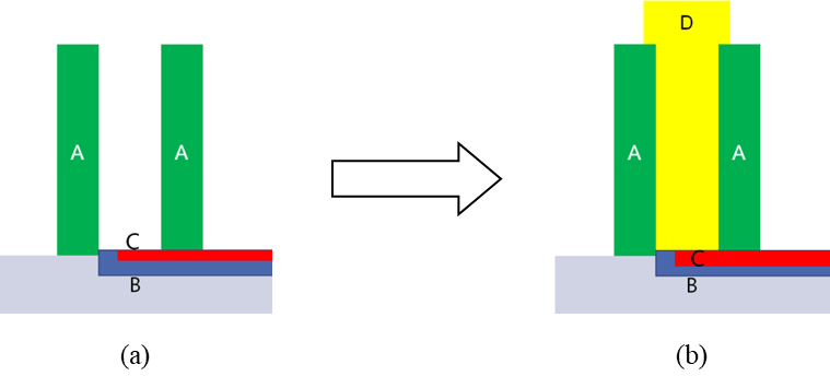
In general, during semiconductor manufacturing process engineers will send wafers to perform various types of test. One of the key purposes of these tests is to achieve key information such as CD (critical dimension) of important structures or devices. And then based on CD information engineers are able to setup R2R control for feedback or feed-forward process control. However, due to complexity of the some device structure and corresponding effect, it is difficult for engineers to conduct accurate prediction of yield impact based on structure CD or overlay fluctuation data. One typical example of this type of structure is contact area in a deep hole. One example of this situation is indicated in Figure 1. B (in gray) is base material. The contact area C (in red) is surrounded by much higher structure A (in green) and planned to have direct contact with D (in yellow).


Figure 1.   
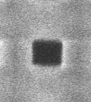
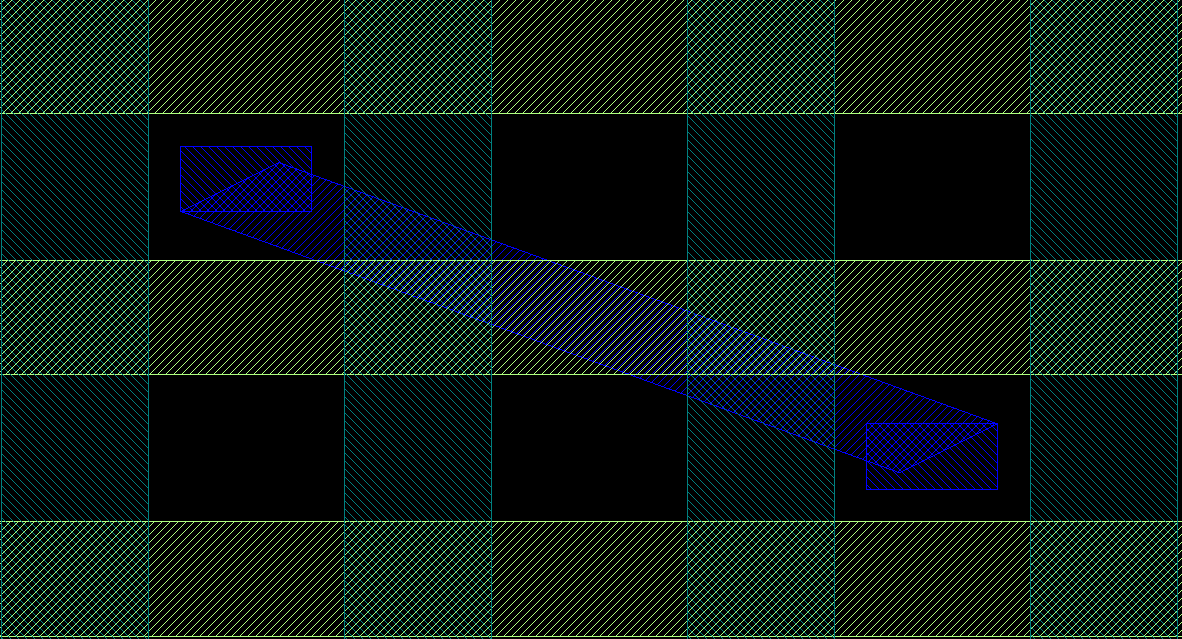
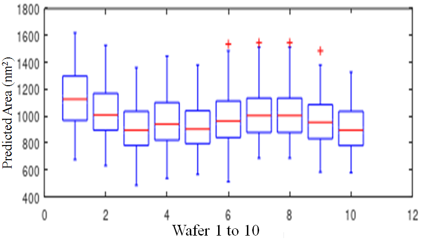
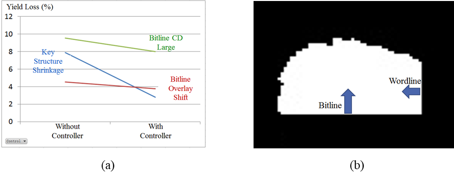
(a) Contact hole structure before contact material D deposited; (b) contact hole structure after contact material D deposited.
The size of contact area has direct impact to contact resistance. Small contact area will result in high contact resistance and result in device malfunction. Due to complexity of manufacturing process, engineers can only get crutial information during the beginning of the process. After surrounding structure stacked, the hole remained to setup electrical contact is too deep to make a measurement based on current measurement instrument technology. Figure 2 shows the measurement result for this type of structure. Besides, due to the contact area is completely unseen, any CD or overlay shifting when surrounding top structure built is difficult for engineer to judge the effect.


Figure 2.   Measurement instrument cannot take clear view of contact area in the deep hole.
This paper proposed a novel type of R2R control strategy as a practical solution to this type of issue. R2R control has been widely used in semiconductor manufacturing industry. The R2R control is commonly based on measuring instrument result. To optimize the control strategy, researchers have tried various types of control algorithm, such as EWMA [1, dEWMA [2]. And in the past 20 years, with popularity of VM (virtual metrology) and the rise of machine learning technology, many more engineers and researchers start to conduct a control strategy based on virtual measurement [3][4][5][6]. However, these new strategies are all focus on information prediction based on equipment sensor data which requires huge data pool and high accuracy of the algorithm.
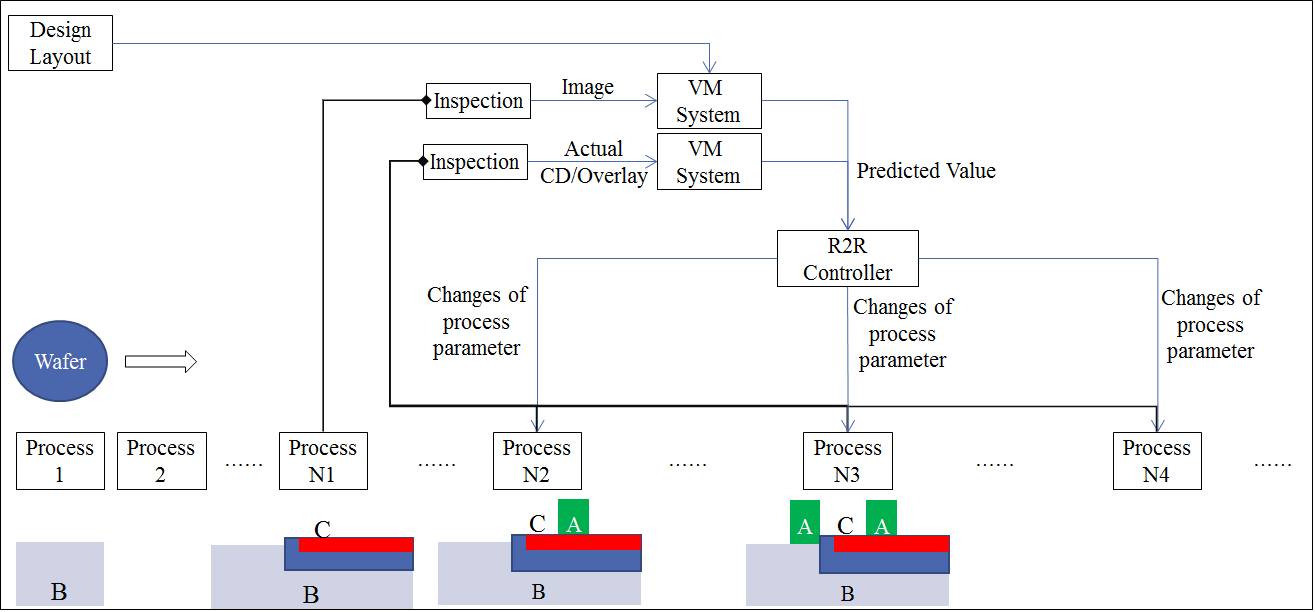
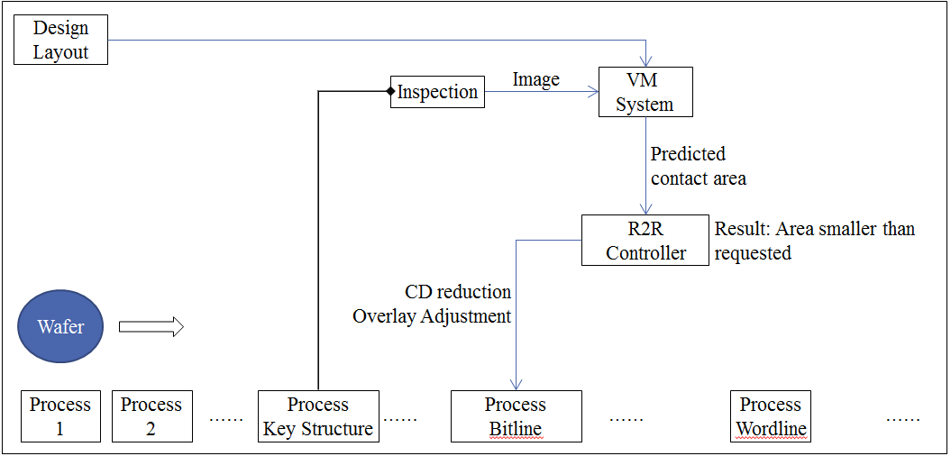
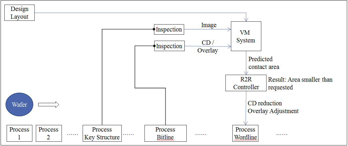
This paper proposed completely different concept of VM. The new type of R2R control strategy is illustrated in Figure 3 below. The VM system will utilize structure information obtained from circuit design document. Based on layout dimension VM system can virtually deploy structure on the inspection image and then generate a new type of virtually measurement data. Associated with new type of metrology data input, a novel feed-forward rolling-wave R2R control plan is formed. Once initial predicted value input, the R2R controller can commend all related subsequent process steps to change process parameter in order to achieve target value. And after subsequent process completed with inspection information (such as CD, overlay), VM system can update the real structure location and then update the R2R controller the latest predicted value. Based on latest predicted value, the R2R controller can re-calculate and send newest process parameter control instruction to the rest of process steps.


Figure 3.   The diagram of new R2R control strategy.
2.   Structure Virtually Deployment Based VM System
2.1.   VM System - Extract Region of Interested
The initial step is to use image processing extract ROI (region of interest). The image below is the AEI (After Etch Inspection) image from SEM (Scanning Electron Microscopy) machine. One can observe the image with noise in Figure 4(a). The noise in the image will cause measurement result inaccurate. In ROI extract stage, the primary task is to remove noise on the image. The paper here is using bilateral filter to remove noise. It’s a complex filter can remove noise while enhance pattern edges [7]. After noise removal the image has sharpened feature. The result can be seen in Figure 4(b).


Figure 4.   SEM inspection image: (a) before bilateral filter; (b) after filter.
The secondary task is to extract the region of interest. One can observe the area with brighter color in the center of the SEM image. This bright area is the area we plan to measure. To fully differentiate our ROI with background, this paper used image binarization with Otsu thresholding technology which is firstly raised by N. Otsu and widely used in image processing area [8].
The outcome after image binarization is displayed in Figure 5: the ROI is colored as completely white while the background is in black.


Figure 5.   ROI extraction result white color is the key structure extracted.
2.2.   VM System - Structure Virtual Deployment
After the ROI is extracted, the next step will be using circuit design to virtually construct the surrounding top structure. The structure layout is shown in Figure 6:


Figure 6.   Layout structure in original design file.
The tilted pattern with similar shape of ROI is our key structure. The key structure is surrounded by other structures. The horizontal lines built over the center of the key structure are defined as bitlines in this paper. The vertical lines are defined as wordlines in this paper. The designed cross over points of wordlines and key structure are located at 1/3 key structure length to the end of the key structure. Based on the design information, the surrounding top structures (bitline and wordlines) will be built in the subsequent process step. The VM system will virtually draw them on the ROI extracted in previous step based on designed position and CD (before bitlines and wordlines are actually constructed).
The result is illustrated in Figure 7. The key structure area not covered by lines is virtually formed contact area which is named as feet area in this paper. To simplify the naming, this paper defines the left area as LF (left feet), while the right area as RF (right feet).


Figure 7.   After virtual structure deploy the 2 feet remains as white.
2.3.   VM System - Contact Area Virtual Measurement
The final step is to extract the LF and RF area size. To obtain the actual area size, the paper uses a simple model below:
(1)
where CA is contact area, N is count of white color pixel, Res is image resolution, unit: nm/pixel.
To further exam the accuracy, the study here uses actual data from manufacturing fabrication center. 10 wafers are sent for VM system. With 315 points measurement, the result of is shown in Figure 8.


Figure 8.   Box plot of 10 wafers result.
3.   Rolling Wave R2R Control Plan
Unlike commonly used R2R control plan the rolling wave R2R control plan is focus on feed-forward control. The case this paper applied has 3 structures related: key structure, bitline and wordline. The key structure, bitline and wordline formation sequence in this study is: Firstly the key structure is formed. Then the bitline is constructed. Finally the wordline is setup. As the wordline setup process step is the final adjustable step for controller, the control plan in this paper is designed to have 2 main logic flows:
3.1.   Contact Area Small before Wordline & Bitline
The issue is mainly caused by key structure shrinkage. The controller will calculate the necessary compensation and request both bitline and wordline to slightly reduce on CD or adjust overlay condition (if one of the feet area is larger than requested). Adjust both bitline and wordline is due to process margin limitation, sometime the area compensation requirement is too large to compensate by bitline only. The logic is illustrated in Figure 9.


Figure 9.   Control logic flow chart for contact area small before wordline & bitline.
3.2 Contact Area Small after Bitline Formed
After bitline actually formed, the VM will update the latest contact area prediction. The controller will calculate the necessary compensation and request wordline to slightly reduce on CD or adjust overlay condition. The logic is illustrated in Figure 10.


Figure 10.   Control logic flow chart for contact area small after bitline formed.
4.   Result & Conclusion
To confirm the outcome of the system, the study here performed trials on real wafers. Due to the contact area is not able to be measure by measurement tools. The study uses final yield to check the correctness of the system. We prepared split conditions of key structure shrinking, bit line overlay shift and bit line CD too large. The chart in Figure 11(a) below shows the yield loss comparison for 3 split conditions with or without controller. From the chart, we can observe the bitline has stronger effect on area correctness. Once bitline is done, wordline can hardly gain area. This scenario has observed on the feet shape in the VM as well. As Figure 11(b) illustrated below, every nm bitline moved has nearly tripled effect compare with wordline movement.


Figure 11.   (a) Yield loss result for 3 split conditions; (b) every nm bitline moved has nearly tripled effect compare with wordline movement.
To summarize statistic result indicates the system has sussesfully adjusted the contact area to correct inline error and achieve less yield loss caused by contact failure.
Acknowledgments
This study is strongly supported by my department manager Haw-Jyue Luo for gently sharing his years of semiconductor manufacturing experience. This research would never be completed without his kindly assistance on inter-department cooperation. Also I would like to thank all my colleagues from JHICC who has selflessly use out-of-office hour to support the experiment and provided insight and expertise.
Acknowledgments
[1] A. Ingolfsson and E. Sachs, "Stability and sensitivity of an EWMA controller", J. Quality Technology, vol. 25, pp. 271-287, 1993.
[2] S. W. Butler and J. A. Stefani, "Supervisory run-to-run control of poly silicon gate etch using in situ ellipsometry", IEEE Trans. Semicond. Manuf, vol. 7, pp. 193-201, 1994.
[3] P. Kang, D. Kim, H.-J. Lee, S. Doh, and S. Cho, “Virtual metrology for run-to-run control in semiconductor manufacturing,” Expert Syst. Appl., vol. 38, no. 3, pp. 2508–2522, 2011.
[4] A. A. Khan, J. R. Moyne, and D. M. Tilbury, “An approach for factory-wide control utilizing virtual metrology,” IEEE Trans. Semicond. Manuf., vol. 20, no. 4, pp. 364–375, Nov. 2007.
[5] A. A. Khan, J. R. Moyne, and D. M. Tilbury, “Virtual metrology and feedback control for semiconductor manufacturing processes using recursive partial least squares,” J. Process Control, vol. 18, no. 10, pp. 961–974, 2008.
[6] F.-T. Cheng, C.-A. Kao, C.-F. Chen, and W.-H. Tsai, “Tutorial on applying the VM technology for TFT-LCD manufacturing,” IEEE Trans. Semicond. Manuf., vol. 28, no. 1, pp. 55–69, Feb. 2015.
[7] Sylvain Paris; Pierre Kornprobst; Jack Tumblin; Frédo Durand, Bilateral Filtering: Theory and Applications , now, 2009.
[8] N. Otsu, "A Threshold Selection Method from Gray-Level Histograms," in IEEE Transactions on Systems, Man, and Cybernetics, vol. 9, no. 1, pp. 62-66, Jan. 1979.
Biography
Chang Xu received the B.Eng. degree in Mechanical Engineering with specialization in Mechatronics from National University of Singapore, Singapore, in 2011, and M.S. degree in Mechanical Engineering from National University of Singapore, Singapore, in 2018. He has 7 years of experience with TFT-LCD manufacturing technology. He is currently working for Fujian Jinhua Integrated Circuit Co., Ltd. (JHICC) in Analysis Technology Department. His research interests include data mining, image processing, pattern recognition, manufacturing, engineering data analysis.
Article and author information
Chang Xu
Publication records
Published: Sept. 18, 2021 (Versions1
References
Journal of Microelectronic Manufacturing