Archive Versions 1 Vol 3 (2) : 20030201 2020
Download
FinFET Performance Enhancement by Source/Drain Cavity Structure Optimization
: 2020 - 03 - 11
: 2020 - 05 - 28
: 2020 - 06 - 08
2525 120 0
Abstract & Keywords
Abstract: Fin field-effect transistor (FinFET) technology has been introduced to the mainstream complementary metal-oxide semiconductor (CMOS) manufacturing for low-power and high-performance applications. However, advanced FinFET nodes are facing significant challenges to enhance the device performance due to the increasingly prominent parasitic resistance and capacitance. In this study, for the first time, we demonstrate methods of enhancing p-channel FinFET (pFET) performance on a fully integrated advanced FinFET platform via source/drain (S/D) cavity structure optimization. By modulating the cavity depth and proximity around the optimal reference point, we show that the trade-off between the S/D resistance and short channel effect, as well as the impact on the parasitic capacitance must be considered for the S/D cavity structure optimization. An extra process knob of applying cavity implant on the desired cavity structure was also demonstrated to modify the S/D junction profile for device performance enhancement.
Keywords: FinFET performance; parasitic resistance and capacitance; source/drain cavity; cavity implant
1.   Introduction
It has been almost a decade since the first fin field-effect transistor (FinFET) technology was commercialized. Owing to the superior electrostatic integrity, FinFET technology has demonstrated significant advantages over conventional planar devices to extend Moore’s law, and is now being adopted by all the leading semiconductor manufacturers for low-power and high-performance applications [1–3]. However, with continuing aggressive technology scaling, the impact of the undesirable parasitic resistance and capacitance becomes increasingly prominent and even outpaces other device aspects at advanced FinFET nodes [4, 5]. Selective epitaxial growth of silicon (Si) and silicon germanium (SiGe) layers in the recessed source/drain (S/D) cavity regions is essential to improve FinFET drive current by reducing the parasitic resistance, but it also raises the parasitic capacitance between the metal gate and S/D electrodes, which may adversely impact the performance at the circuit level [6–9]. Therefore, the trade-off between the parasitic resistance and capacitance must be considered to optimize FinFET performance. In this study, for the first time, we report the impact of the recessed S/D cavity structure on p-channel FinFET (pFET) performance on a fully integrated advanced FinFET platform, and we demonstrate an extra process knob of applying an ion implantation process after the cavity formation for pFET performance enhancement.
2.   FinFET S/D Cavity Formation
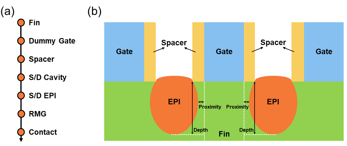
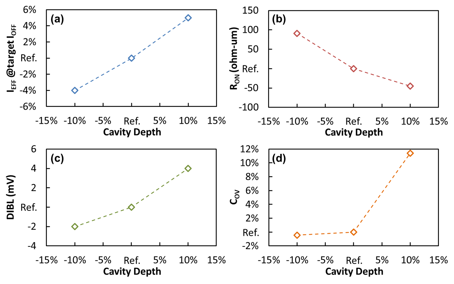
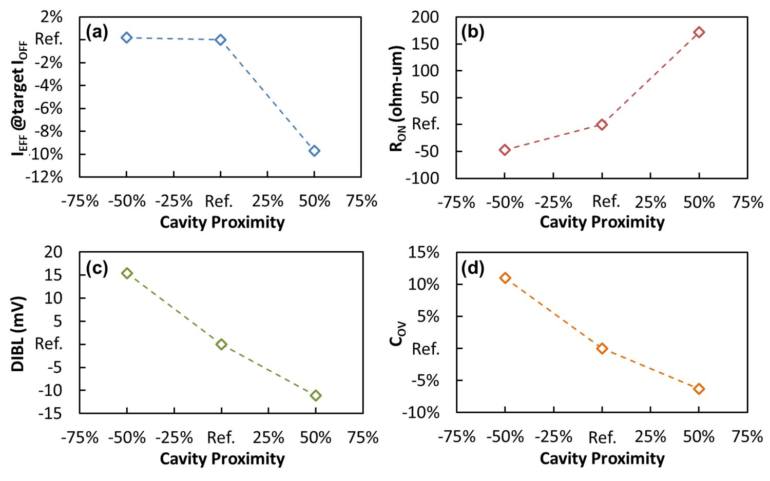
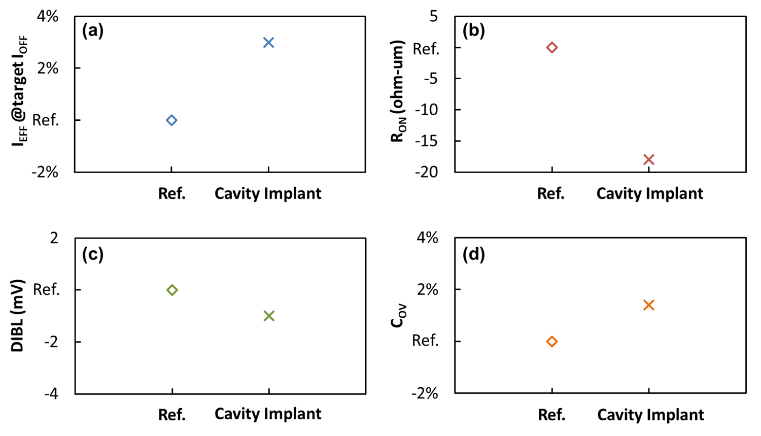
A fully integrated advanced bulk FinFET complementary metal-oxide semiconductor (CMOS) platform was adopted to perform this study. Figure 1(a) depicts the schematic process flow of advanced bulk FinFET fabrication [10]. After the formation of fin and dummy gate structures, low-dielectric constant (low-k) films were deposited over the wafer using an atomic layer deposition (ALD) process to form gate sidewall spacers [11, 12]. A reactive ion etching (RIE) process was then applied to form recessed cavity structures in the S/D regions for the subsequent epitaxy (EPI) processes. The S/D cavity formation process was comprised of three steps: removing the spacer from the top of the fin, recessing the exposed fin by an anisotropic etching process, and setting the final cavity geometry by an isotropic etching process. In the first step, the amount of the spacer pulldown on the fin is a critical parameter to control the lateral width of S/D EPI [13]. The second anisotropic etching step is the main step to recess the fin vertically along the gate sidewall spacer, and the third isotropic etching step is the final step to further etch the fin vertically and laterally under the spacer to achieve the desired cavity geometry. Figure 1(b) shows the typical cavity profile of a pFET device, the cavity depth is defined as the distance from the top of the fin to the bottom of the cavity, and the cavity proximity is defined as the distance from the lateral edge of the cavity to the edge of the gate. Following the cavity formation, S/D EPI processes were optimized according to the cavity geometry to achieve the desired EPI geometry, then the replacement metal gate (RMG) and metal contact formation processes were performed to complete FinFET fabrication. In this study, pFET devices with a range of cavity depth and proximity targets were fabricated by modifying the etching time of each individual step of the cavity formation process, in-situ boron (B) doped SiGe EPI was formed in the recessed cavity regions as the stressor to enhance the hole mobility [14–17]. The impact of applying a low-energy B ion implantation process in the S/D cavity regions before SiGe EPI formation was also investigated.


Figure 1.   (a) Schematic process flow of advanced bulk FinFET fabrication. (b) Schematic pFET device structure along the fin, the S/D cavity depth and proximity are also shown.
3.   Device Characteristics
The pFET devices under study were based on a dense 2-fin standard logic cell, and the electrical tests were performed at the metal one (M1) level with the supply voltage Vdd = 0.75V. Device on-resistance (RON) was measured at the linear region with the overdrive gate voltage of 0.7V, and drain-induced barrier lowering (DIBL) was measured at a fixed current density of 10nA/um. To decouple the threshold voltage (VT) impact, effective current (IEFF) at the target off-current density (IOFF) of 11nA/um was characterized as the device metric for transistor current drivability. Since the gate electrode is wrapped around the channel in FinFET devices, the resistance and current in this study were normalized by the effective gate width of 91nm per fin. In addition, a capacitor array structure at zero gate bias was adopted to characterize the overlap capacitance (COV) between the gate and S/D electrodes through the gate oxide and sidewall spacer. COV is a clear indicator of the S/D junction placement with respect to the gate electrode, and it is a major component of the overall effective capacitance, therefore COV should also be considered in order to optimize the performance at the circuit level.
3.1.   Cavity Depth
Cavity depth mainly impacts the S/D junction profile in the vertical direction. Figure 2(a)-(d) show the pFET performance response with the cavity depth modulation of +/-10% with respect to the optimal reference point, and the cavity proximity was kept the same. IEFF was enhanced by 5% with 10% cavity depth increase from the reference, and the performance gain was driven by 45ohm-um RON reduction despite slightly degraded short channel effect indicated by 4mV higher DIBL, however COV was increased by 11.4% and that was not desirable for the circuit-level performance. Consistently, 10% cavity depth reduction from the reference led to 4% IEFF degradation driven by 91ohm-um higher RON. In summary, as the cavity depth is increased towards the bottom of the fin, the current drivability is enhanced from S/D resistance reduction. However, if the cavity depth is further increased, the short channel effect becomes prominent and eventually results in device performance degradation instead, and the significant increase in the parasitic capacitance degrades the circuit-level performance as well.


Figure 2.   (a) IEFF at target IOFF, (b) RON, (c) DIBL and (d) COV of pFET devices as a function of cavity depth.
3.2.   Cavity Proximity
Cavity proximity is another design knob to enhance the device performance by optimizing the trade-off between the S/D resistance and short channel effect. Figure 3(a)-(d) show the pFET performance as a function of cavity proximity of +/-50% with respect to the optimal reference point, and the cavity depth was kept the same. Compared to the reference, 50% larger cavity proximity degraded IEFF by 9.7%, which was mainly driven by 172ohm-um higher RON. On the other hand, as the cavity proximity was reduced by 50% from the reference, the penalty from short channel effect indicated by 15mV higher DIBL overweighed RON reduction of 47ohm-um and ultimately limited IEFF improvement to as low as 0.2%. Moreover, COV demonstrated a strong correlation with cavity proximity modulation as shown in Figure 3(d), indicating S/D junction movement in the lateral direction with respect to the gate electrode. Compared to the reference, COV was increased by 11% as the S/D was placed closer to the gate electrode with 50% smaller cavity proximity, and COV was reduced by 6.3% as the S/D was placed further away from the gate electrode with 50% larger cavity proximity. Therefore, even though the 50% smaller cavity proximity demonstrated slight improvement in the current drivability, the parasitic capacitance increased significantly and resulted in the circuit-level performance degradation.


Figure 3.   (a) IEFF at target IOFF, (b) RON, (c) DIBL and (d) COV of pFET devices as a function of cavity proximity.
3.3.   Cavity Implant
Another process knob explored in this study is the cavity implant, which is an ion implantation process applied in the S/D cavity structure before the EPI formation using the same type of dopant as applied in the S/D later in the process flow. Depending on the implant energy, dose and tilt angle, the cavity implant can effectively deepen the junction profile towards the bottom of the fin and/or extend it in the lateral direction under the spacer. Unlike the cavity depth or proximity optimization by tuning the etching process, cavity implant is a relatively friendly process that does not involve any structural change, and it serves as an extra knob to enhance the device performance on the desired S/D cavity structure. Figure 4(a)-(d) show the performance enhancement on a pFET device with the cavity implant in comparison to a reference has the same cavity depth and proximity without the cavity implant. The cavity implant was performed at a dose of about 1014 atoms/cm2 and a kinetic energy of about 1keV with ions drawn from B, and the tilt angle was set at zero degree to deepen the S/D junction profile with minimal extension in the lateral direction. As the result of the cavity implant, IEFF was improved by 3% driven by 18ohm-um RON reduction with comparable short channel effect, and COV only showed a slight increase of 1.4%.


Figure 4.   (a) IEFF at target IOFF, (b) RON, (c) DIBL and (d) COV of pFET devices with and without cavity implant.
4.   Conclusion
In this study, the impact of the recessed S/D cavity structure on the performance of pFET devices on a fully integrated advanced FinFET platform is reported for the first time. S/D cavity depth and proximity were modulated around the optimal reference point by tuning the cavity formation etching process, and an extra process knob of applying cavity implant on the desired cavity structure was also demonstrated to modify the S/D junction profile. Device characteristics were discussed and guidelines to enhance the device performance by optimizing the S/D cavity structure were provided considering the trade-off between the S/D resistance and short channel effect, as well as the impact of the parasitic capacitance on the circuit-level performance.
[1] C. Auth et al., “A 22nm high performance and low-power CMOS technology featuring fully-depleted tri-gate transistors, self-aligned contacts and high density MIM capacitors,” 2012 Symposium on VLSI Technology(VLSIT) , pp. 131-132, Honolulu, HI (2012).
[2] S. Natarajan et al., “A 14nm logic technology featuring 2nd-generation FinFET, air-gapped interconnects, self-aligned double patterning and a 0.0588 µm2 SRAM cell size,” 2014 IEEE International Electron Devices Meeting (IEDM), pp. 3.7.1-3.7.3, San Francisco, CA (2014).
[3] C. Auth et al., “A 10nm high performance and low-power CMOS technology featuring 3rd generation FinFET transistors, Self-Aligned Quad Patterning, contact over active gate and cobalt local interconnects,” 2017 IEEE International Electron Devices Meeting (IEDM), pp. 29.1.1-29.1.4, San Francisco, CA (2017).
[4] T. An et al., “Performance optimization study of FinFETs considering parasitic capacitance and resistance,” JSTS: Journal of Semiconductor Technology and Science 14 (5), 525 (2014).
[5] B. R. Huang et al., “Investigation of parasitic resistance and capacitance effects in nanoscaled FinFETs and their impact on static random-access memory cells,” Japanese Journal of Applied Physics 56 , 04CD11 (2017).
[6] C. R. Manoj et al., “Impact of fringe capacitance on the performance of nanoscale FinFETs,” IEEE Electron Device Letters 31 (1), 83 (2010).
[7] C. Sohn et al., “Analytic model of S/D series resistance in trigate FinFETs with polygonal epitaxy,” IEEE Transactions on Electron Devices 60 (4), 1302 (2013).
[8] F. H. Meng et al., “Effect of three-dimensional current distribution on characterizing parasitic resistance of FinFETs,” Japanese Journal of Applied Physics 55 , 04ED16 (2016).
[9] J. Kim et al., “Modeling of FinFET parasitic source/drain resistance with polygonal epitaxy,” IEEE Transactions on Electron Devices 64 (5), 2072 (2017).
[10] S. Narasimha et al., “A 7nm CMOS technology platform for mobile and high performance compute application,” 2017 IEEE International Electron Devices Meeting (IEDM), pp. 29.5.1-29.5.4, San Francisco, CA (2017).
[11] T. Han et al., “Forming a more robust sidewall spacer with lower k (dielectric constant) value,” 2017 China Semiconductor Technology International Conference (CSTIC), pp. 1-3, Shanghai (2017).
[12] M. Gu et al., “Hybrid low-k spacer scheme for advanced FinFET technology parasitic capacitance reduction,” Electronics Letters 56 (10), 514 (2020).
[13] H. Lo et al., “Performance boost using spacer-confined cavity for advanced FinFET technology,” Semiconductor Science and Technology 34 , 015012 (2019).
[14] M. Choi et al., “14nm FinFET stress engineering with epitaxial SiGe source/drain,” 2012 International Silicon-Germanium Technology and Device Meeting (ISTDM), pp. 1-2, Berkeley, CA (2012).
[15] G. Wang et al., “Integration of highly-strained SiGe materials in 14nm and beyond nodes FinFET technology,” Solid-State Electronics 103 , 222 (2015).
[16] N. A. F. Othman et al., “Impact of channel, stress-relaxed buffer, and S/D Si1−xGex stressor on the performance of 7-nm FinFET CMOS design with the implementation of stress engineering,” Journal of Electronic Materials 47 , 2337 (2018).
[17] S. Shintri et al., “Effects of high in-situ source/drain boron doping in p-FinFETs on physical and device performance characteristics,” Materials Science in Semiconductor Processing 82 , 9 (2018).
Article and author information
Man Gu
man.gu@globalfoundries.com
Wenjun Li
Haiting Wang
Owen Hu
Publication records
Published: June 8, 2020 (Versions1
References
Journal of Microelectronic Manufacturing