We have used a NA of 0.33 and 0.9-0.7 Quasar 35° partial coherence setting with a typical 30 nm thick Chemically Amplified photoresist (CAR). Figure 2 shows the shadowing effect at different slit positions, 0, -13 mm, and 13 mm. In order to avoid the stochastic printing failures
[2], the anchor point is set at 36 nm pitch and 18 nm ADI Critical Dimension (CD) and the corresponding reasonable Exposure Latitude (EL) must be ≥ 18%
[3]. At the center of the exposure slit, the pattern shift in -Y direction results from shadowing effect is about 1.52 nm
[1] for pattern oriented along X direction, while that shift of the pattern along Y direction is 0 nm. When slit position is not in the center, patterns that orients either along X or Y direction will have shift. However, the shift of the pattern along Y direction is much smaller than that of pattern along X direction. With the slit position away from center, the shift of the pattern along X direction becomes smaller and that of the pattern along Y direction becomes larger.
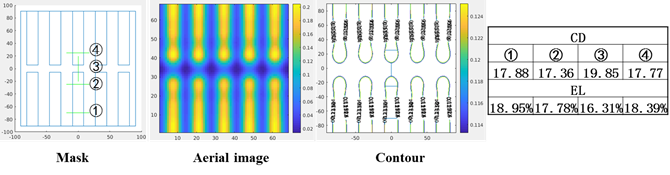
Figure 2.
Shadowing Effect at slit=0, -13 mm, 13 mm for 36 nm pitch and 18 nm ADI CD. The simulation data of typical design rule patterns are displayed in Table 1(a) and Table 1(b). These data include simulated EL and CD and recommended EL and CD. For Table 1(a), the patterns are, from left to right, tip-to-line(TtL), tip-to-tip (TtT) within dense pattern, TtT, TtT on one side of dense pattern, staggered TtT, short bar on one side of wider line, minimum isolated area on one side of wider line. For Table 1(b), the patterns are, from left to right, isolated short bar on one side of dense line/space, minimum isolated area on one side of dense line/space, left line of isolated tri-lines (the right two lines are represented by hollow bars), center line of isolated tri-lines (the two edge lines are represented by hollow bars), right line of isolated tri-lines (the left two lines are represented by hollow bars), left line of isolated bi-lines (the right line is represented by a hollow bar), right line of isolated bi-lines (the left line is represented by a hollow bar). Recalling in 193 nm immersion lithography, according to the setting of typical design rules, the EL for 2D patterns, such as TtT and TtL is ≥ 10%, which is smaller than the EL for the most dense line and space patterns, say ≥13% for the metal and ≥18% for the gate
[4]. For 2D patterns in EUV lithography, taking EUV stochastics impact into account,EL for the line and space patterns are recommended to be at least 18%, therefore, EL for the 2D patterns must be upgraded to ≥ 13%, In the following sections, the simulation results of several patterns are discussed. In order to obtain acceptable process window data, we have added appropriate optical proximity correction (OPC) which is not shown here.
Table 1(a) The simulation data of typical design rule 2D patterns
Table 1(b) The simulation data of typical design rule 2D patterns 2.1 The Simulation of Typical Design Rule Patterns with EUV Photolithographic Process
Figure 3.
The mask and simulation results of TtT pattern. A typical mask of TtT pattern is depicted in Figure 3. The pattern pitch is 36 nm and trench CD on mask is 18 nm with TtT gap CD equal to 11.2 nm. From the simulation results, line cut ① as the anchor point, taking EUV stochastics impact into account, EL must be ≥ 18%, ③ is the TtT line cut which EL must be ≥ 13%. Line cut ② and ④ is the trench width near the tip, which is used as monitor of optical proximity effect. From our simulation, we have found that the CD and EL at all line cut positions satisfy our target requirement with TtT CD close to target of 20 nm.
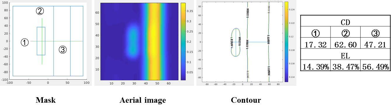
Figure 4.
The mask and simulation results of minimum isolated area on one side of wider line. Shown in Figure 4 is another situation. The mask CD of isolated area is 21 nm along X direction (at line cut ① position) and 72 nm along Y direction (at line cut ② position) and the wider trench next to the isolated area has a CD of 43.2 nm (at line cut ③ position). In order to achieve an EL more than 13%, we have found that the minimum area is about 5 times that of minimum pixel squared, i.e. 5×18×18 nm2, with about 17.5 nm contour CD at line cut ① position.
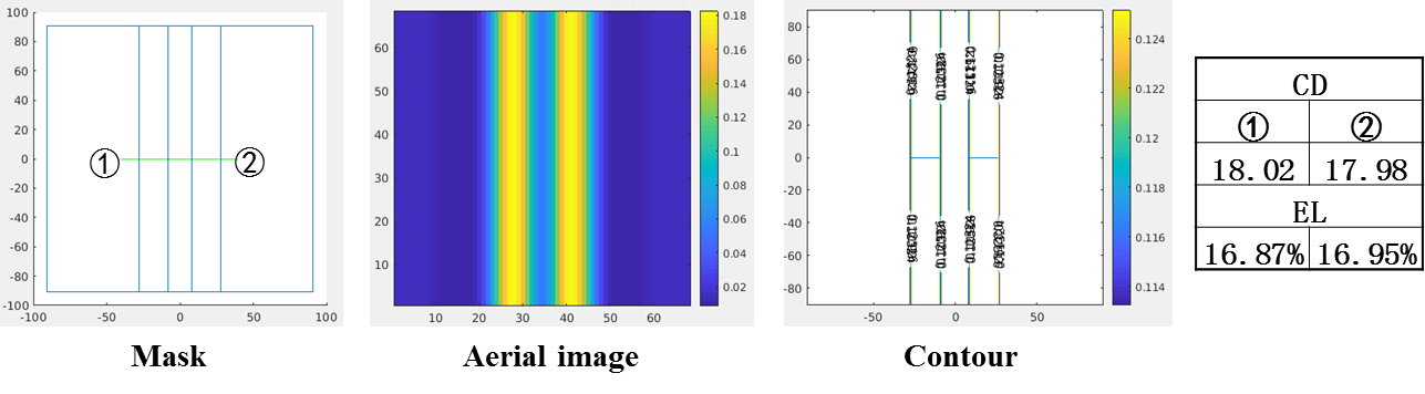
Figure 5.
The mask and simulation results of bi-lines. Figure 5 described another pattern, which is one of the most challenging patterns in photolithography: the bi-lines. For process window consideration, we have found that the minimum pitch can also be kept at 36 nm, while a mask bias of 1.8 nm must be used compared to anchor pattern.
2.2 Increased Impact of Aberration in EUV Lithography
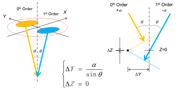
Figure 6.
Schematic diagram of coma induced pattern shift as a function of illumination pupil position. From Figure 6, we can see that pattern shift caused by aberration is inversely proportional to NA. Because NA for EUV is much smaller than that for 193 nm immersion, its horizontal position is more sensitive to odd aberration. Then, compared to aberration impact from 193 immersion, aberration from 0.33NA EUV exposure tools needs be controlled to a smaller extent. In the following sections, the pattern shift owing to Transverse Coma aberration of 2D patterns, as mentioned in Table 1(a) and 1(b), is discussed.
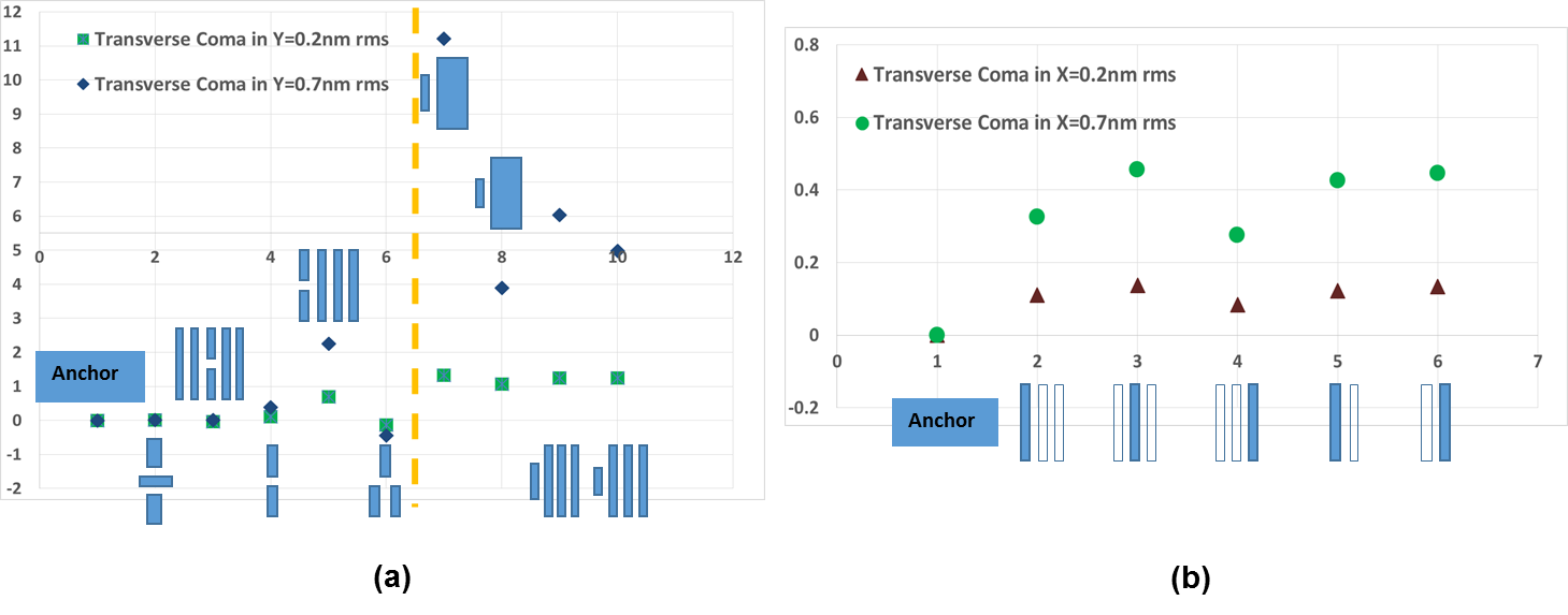
Figure 7.Pattern shift caused by Transverse Coma aberration of 0.2 nm rms and 0.7 nm rms,(a): Transverse Coma in Y (Z8), (b): Transverse Coma in X (Z7). For different 2D patterns, the transverse aberration (Coma) in X- or Y-direction of 0.2 nm
root-mean-square (rms) and 0.7 nm rms are shown in Figure 7. As expected, the OVL must be controlled to within ± 2.5 nm in 5 nm Logic Process. When the transverse Coma in Y (Z8) is 0.2 nm rms shown in Figure 7(a), the pattern shift for typical 2D patterns contributing to OVL budget is in the range of -1~+1 nm, which is reasonable. For bi-lines and tri-lines shown in Figure 7(b), these pattern shifts are all in the range of 0.6 nm under typical transverse Coma in X(Z7) of 0.2 nm rms and 0.7 nm rms. Next, we will describe in detail pattern shifts owing to Coma aberration of three patterns.
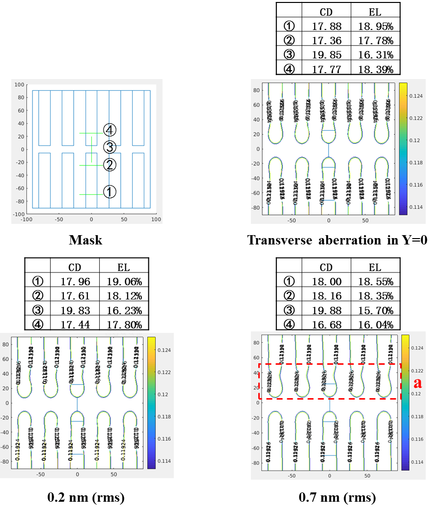
Figure 8.
Pattern shift caused by Transverse aberration in Y of 0.2 nm rms and 0.7 nm rms for TtT pattern. The mask pitch is 36 nm and mask trench CD is 18 nm with TtT gap CD of 11.2 nm. For TtT pattern shown in Figure 8, a transverse coma in Y-direction of 0.7 nm rms is found to result in a pattern shift and cause a distortion of the tips: necking on the “a” side.
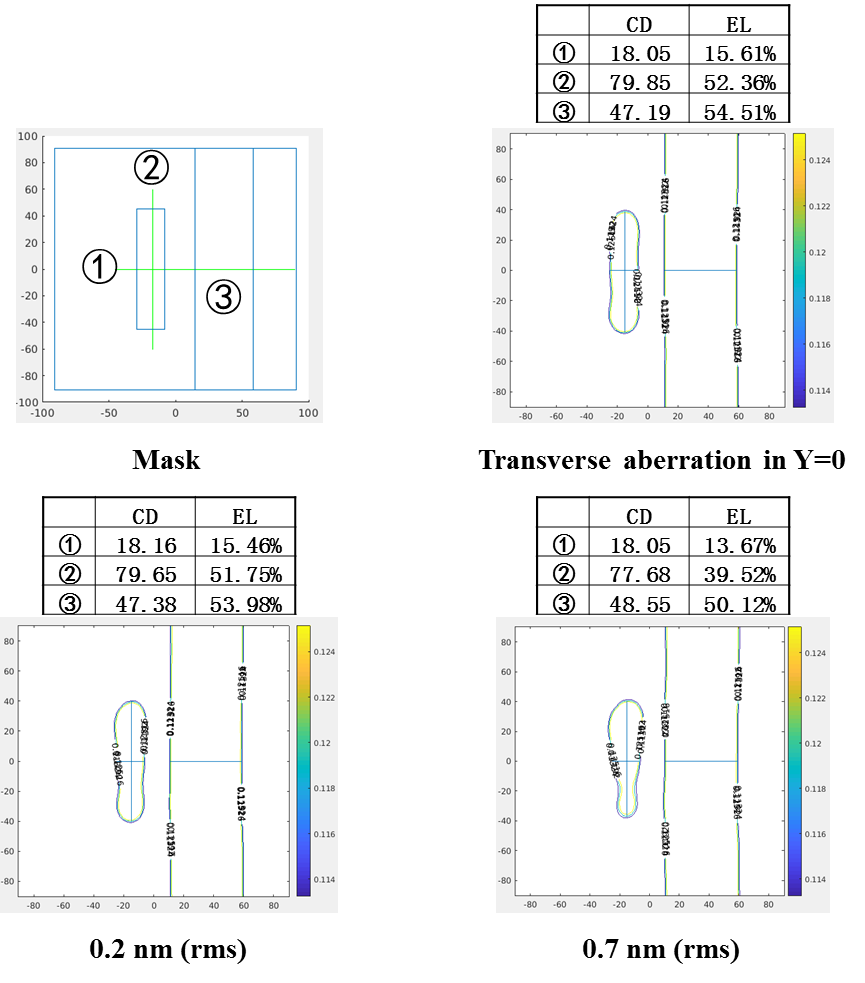
As shown in Figure 9, the mask CD of isolated area is 21 nm along X direction (at line cut ① position) and 90 nm along Y direction (at line cut ② position) and the wider CD next to the isolated area is 43.2 nm (at line cut ③ position). For isolated pattern, the aberration can not only cause the pattern shift and but also result in significant distortion, especially in the case when the aberration is 0.7 nm rms.
Figure 9.
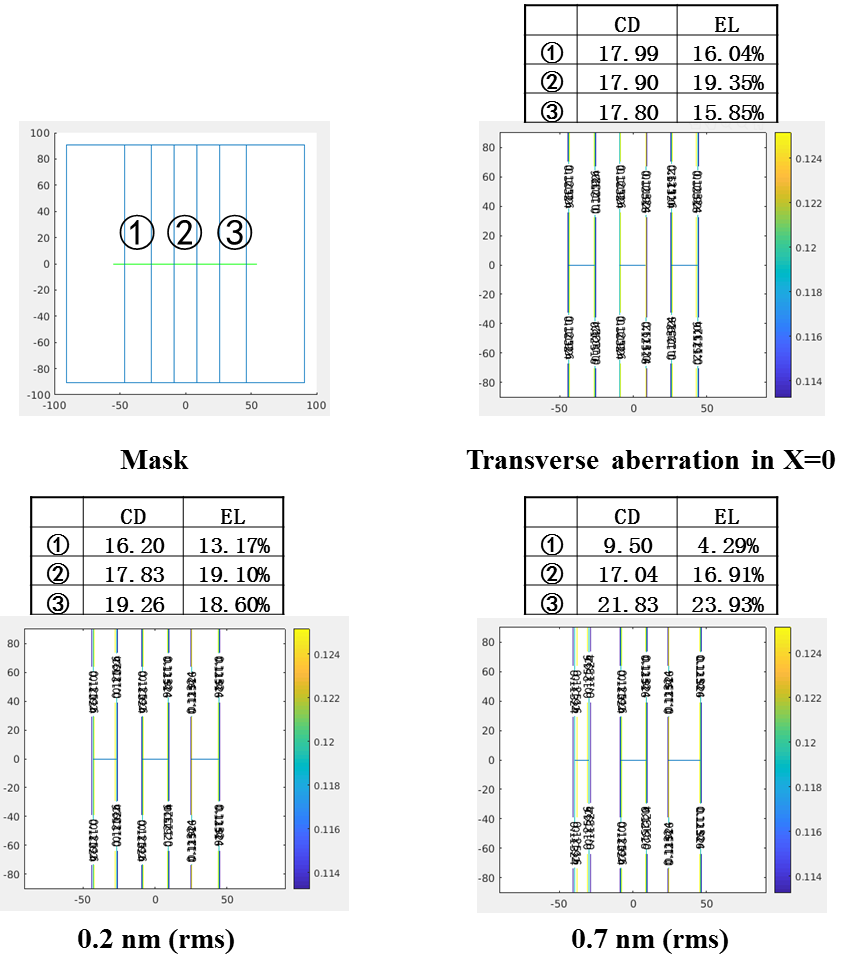
Pattern shift caused by Transverse aberration in Y for short bar on one side of wider line. For isolated tri-lines shown in Figure 10, a mask bias of 3 nm for the two edge trenches have been used compared to the center trench. The transverse aberration can cause pattern shift and cause CD and EL change asymmetrically around the center trench. The CD of the left line is smaller by more than about 10% and 50% with 0.2 nm and 0.7 nm rms aberration, respectively.
Based on above simulation results, rms aberration for EUV lithography with 0.33NA needs to be kept under 0.2 nm while the rms aberration for 193 nm immersion exposure tools are usually kept under 1 nm
[5]. All these impact including in CD, EL, and pattern shape fidelity must be compensated by OPC.
Figure 10.
Pattern shift caused by Transverse aberration in X of 0.2 nm and 0.7 nm rms for tri-lines.