Research Article Archive Versions 2 Vol 2 (3) : 19020305 2019
Download
Current Status of the Integrated Circuit Industry in ChinaEDA Industry Review
: 2019 - 08 - 22
: 2019 - 09 - 29
3529 94 0
Abstract & Keywords
Abstract: China's IC industry has been flourishing in recent years, huge market demand together with government investments are the major driving forces for this development. The status and development momentum of the Chinese IC industry also attracted wide interest and attention of international counterparts. A group of domestic IC experts are invited by the JoMM to write a series of articles about China's IC industry, including the history, current status, development, and related government policies. Information in these articles is all from public data from recent years. The purpose of these articles is to enhance mutual understanding between the Chinese domestic IC industry and international IC ecosystem.
Keywords: EDA; China
1.   Situation of EDA Industry
1.1.   Global Status of EDA Industry
The integrated circuit industry chain mainly consists of three parts: design, manufacturing, packaging and testing. These three parts determines the quality of the integrated circuit. Behind these there are three more fundamental factors, including equipment, materials and EDA tools. These are more fundamental and strategically supportive elements for the whole integrated circuit industry.
Specifically, EDA is the lifeblood of the development of the integrated circuit industry, which can be inferred from two recently occurred incidents. The first incident refers to the sanction on Huawei, ZTE and other companies by the United States government, in which EDA tools became a critical point. The second is the Electronic Renaissance Program launched by the United States in 2017 which included the advanced EDA technology research in the first batch supported projects. These validates the importance of EDA tools.
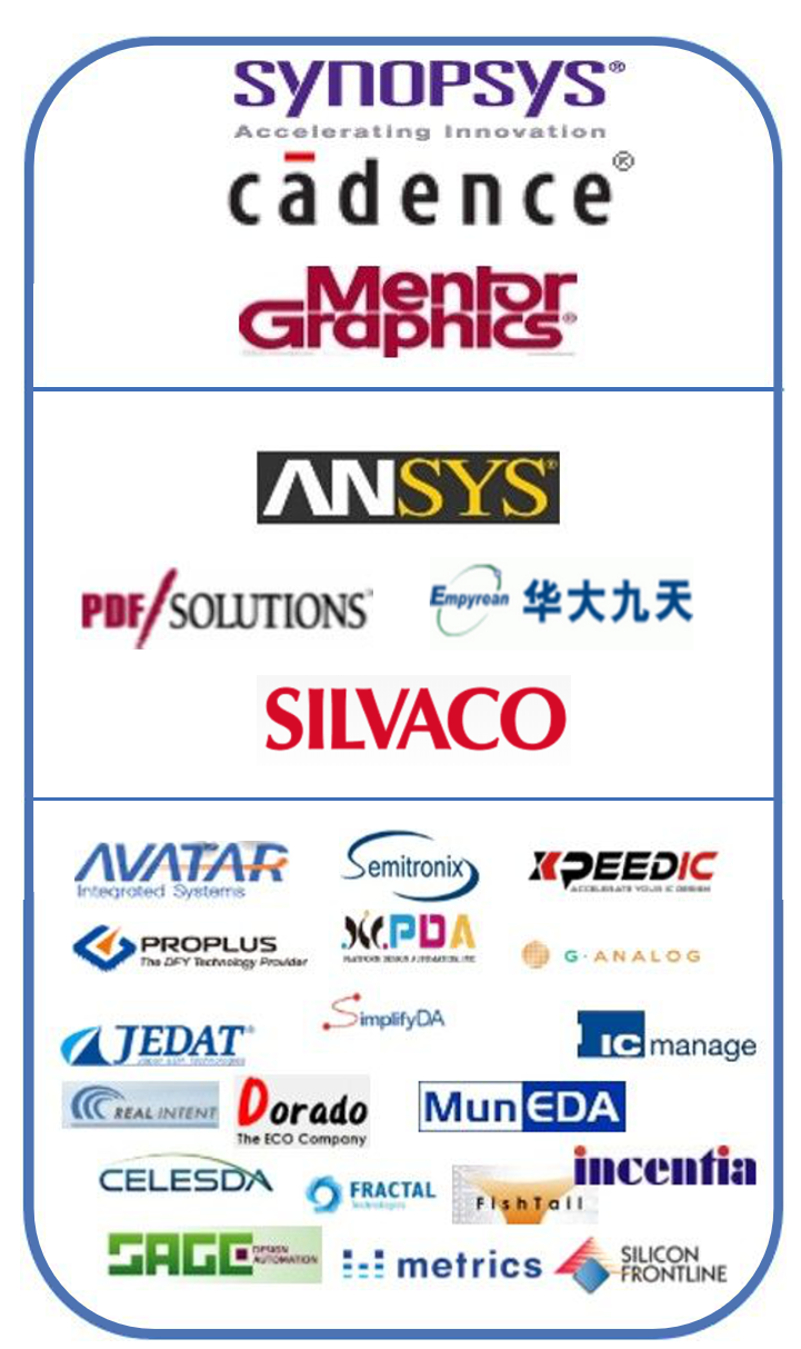
From the perspective of the global EDA industry, there are about sixty or seventy EDA vendors in the world. However, six EDA companies in the United States are dominating the EDA field, which take up 95% of the global market. As shown in Figure 1, the first-tier includes three US companies, Synopsys, Cadence and Mentor, which deliver complete, total-featured, full-process products. They have absolute advantages in some areas. The revenue of each company exceeds 100 million US dollars, accounting for approximately 80% of the global market; in the second-tier, US ANSYS, PDF SOLUTIONS, SILVACO and Empyrean Software in China have a full-process basis product in some specific areas. They have the leading technology in local areas, accounting for approximately 15% of the global market. In addition, there are more than 50 small EDA companies in the third-tier. They use the point tools to make annual revenues of less than 20 million US dollars.
In 2018, domestic EDA sales amounted to approximately 500 million US dollars (about 3.3 billion yuan), accounting for 8% of the global market, while domestic EDA tools sales of 340 million yuan, accounting for 10% of the domestic EDA market. It can be inferred that the Chinese EDA tools are mainly from the United States. If there is a competition between China and the United States, or a trade war, etc., EDA will always be a fatal problem. If this problem keeps unsolved, China has to face the risk of being banned the United States. This case is different from other fields, because alternative equipment, materials and supplies can be found from other countries, but EDA is only available from U.S. based vendors.
At present, there are more than a dozen EDA companies in China, and many people are trying to do related work. According to the statistics, there are about six or seven hundred people working in local EDA firms. However if marketing and technical support people are excluded, the number of actual EDA research and development drops to 500. Therefore, the talents in the domestic EDA field are particularly rare.


Figure 1.   Global Status of EDA Industry.
1.2.   History of Chinese Local EDA Industry
Since the mid-to-late 1980s, China has invested in the research and development of the EDA industry. At that time, the high-tech fields in China, including integrated circuits, were limited in the embargo of COCOM (Coordinating Committee for Export to Communist Countries), and development was greatly constrained. In order to better develop the integrated circuit industry in China, in 1986, 17 state units across the country were mobilized, and more than 200 experts gathered in the former Beijing IC Design Center to develop China's independent integrated circuit computer-aided design system, the Panda System.
After years of hard work, the first domestic EDA Panda system was finally released in 1993. In 2001, the domestic IC design firm launched Empyrean system to explore the overseas market while serving local demand. In 2009, a new company, Empyrean was established to promote the development of domestic EDA.
Although the domestic EDA industry has not achieved commercial success due to various reasons, during the trail, many EDA vendors were born in China. At present, there are about a dozen EDA companies in China as shown in Figure 2.


Figure 2.   Status of Chinese local EDA companies.
1.3.   Characteristics of EDA Industry
EDA industry are mainly features with the following characteristics:
(1) It’s an oligopoly market, the technical difficulty is relatively high. Basically, the first place gains profits, the second place makes break even, the third place loses money. If the company could not make the top two in the industry, there is no chance for it to make profit. The company must hold extremely high technology to meet the demand of the chip products development.
(2) The investment cycle of the EDA industry is relatively long, and the output is relatively slow, requiring continuous capital investment. Basically, it takes about 6 years to develop an EDA tool to truly make a market-approved product that can be applied in the market.
(3) It needs the establishment of an industrial ecosystem for EDA and full support from the upstream and downstream of the industry chain. EDA plays the role of the bond and bridge between manufacturing and design, which means it needs support from manufacturing and design.
(4) The development of EDA industry depends on talents. At present, there is a severe shortage of talents in the domestic EDA field, including both junior and senior levels.
(5) The development of the EDA industry requires mergers and acquisitions. The Big Three in the EDA field are all grown through mergers and acquisitions.
1.4.   Gap with the international EDA industry
Domestic EDA has been exploring and advancing in the ups and downs for a long time. Even though the domestic EDA industry has achieved some achievements, there is still a gap from the international leading firms. There are three main aspects of the gap: (1) Lacking of critical tool module of digital chip designing, unable to support the whole process design of digital chip; (2) Insufficient support for advanced process technology node, only few tools have capability to support 14nm, 7nm, 5nm technology node. (3) Insufficient investment in technology. (4) Insufficient investment in capital. The specific introduction is as follows.
1) The product is not complete enough, especially in the digital circuit, the overall system lacks digital chip design core tool module, and cannot support the full design flow.
Take Empyrean as an example. They only make one-third of the products in this digital circuit field, and two-thirds need make up. An important reason for this situation is that there are not enough engineers to support all-round research and development. Experts from industry, academia and research circles have reached consensus that if China wants to make the whole set of EDA tools, it is not about individual domestic manufacturer, but needs a variety of cooperation.
2) Because of the lacking of integration with advanced technology, domestic EDA tools are not enough for advanced process support.
In the modern integrated circuit industry, the bridge between chip design and manufacturing is very important, EDA plays such a role of bridge. However domestic enterprises have two insurmountable gaps in this docking: on the one hand, domestic EDA vendors have few opportunities to access advanced technologies, which limits their technological advancement. It is understood that the world's leading fabs, such as TSMC and Samsung, will first introduce international cash companies such as Cadence and Synopsys to develop new technologies. Domestic EDA vendors are not valued. They are unable to obtain relevant support from foreign manufacturers. In the long run, the gap between the technology accumulation of domestic EDA companies and international advanced companies will gradually expand.
On the other hand, the shortcomings of the domestic industry in the PDK (Process Design Kit) also has some negative effects on the development of domestic EDA. The PDK contains various documents related to process and device. It is the key to the successful production of the designed chip in the fab. It is the bridge between the IC design company, the foundry and the EDA manufacturer. The lacking of PDK in domestic manufacturers has affected the development of the domestic EDA industry to some extent.
3) Insufficient investment in professional talents
The shortage of professional talents is a key factor limiting the development of domestic EDA. The weak R&D team is difficult to support the massive task of attacking. The root cause of this appearance is the industry's insufficient investment in EDA. There are about 1,500 EDA software development engineers in China, but the number of engineers working in local EDA companies and research units add up to less than 300. Most of the others work in the three international giants. And looking at the global market, comparing to Synopsys with more than 7,000 R&D employees (over 5,000 engaged in EDA, others focused in IP), the gap is even more significant.
4) Less investment in R&D
Among the current local EDA companies, even the largest team and the longest-established firm Empyrean, they have spent only a few hundred million yuan on R&D in the past decade. While foreign advanced competitors invest billions of yuan each year in product research and development (Synopsys' R&D investment in 2017 is about 810 million U.S. dollars, and in 2018 it is more than 1 billion U.S. dollars). Compared with this huge number, domestic EDA company's research and development funds is almost negligible. If domestic EDA wants to further develop, it is imperative to increase capital investment.
2.   Introductions of Chinese Local EDA Companies
2.1.   Empyrean Software
2.1.1.   Introduction
Empyrean Software is established in June 2009 and is a secondary enterprise in the IC business segment of China Electronics Corporation; (CEC). Focusing on providing professional EDA software, IP products and related solutions, Empyrean Software is the largest and most powerful EDA enterprise in China. It is the supporting unit of the National Engineering Research Center for Large Scale Integrated Circuit CAD, and is responsible for the research and development of domestic EDA software. Empyrean Software launched the silicon intellectual property (IP) and design services business in 2012. The number of people in Empyrean Software’s technical team is about 150, more than 80% of which have Master’s or Doctor’s degrees, including three national “Thousand Talents” experts. The headquartered is in Beijing, wholly-owned subsidiaries are in Nanjing and Chengdu, sales department are in Shanghai, Shenzhen and overseas.
Empyrean Software’s predecessor is the EDA department of China Huada IC Design Group Co., Ltd. The company's development history dates back to 1986. China has concentrated more than 100 experts and scholars in the industry, and has taken national efforts to carry out technical research. In 1993, it officially released the first EDA tool with independent intellectual property rights in China - Panda ICCAD. The system won the first prize of the National Science and Technology Progress Award and broke the foreign EDA software blockade in mainland China, making China one of the few countries in the world that can provide independent intellectual property EDA tools. In 2009, China Huada IC Design Group Co., Ltd. and SDIC High-Tech Investment Co., Ltd. jointly invested to separate the EDA department of Huada and established Empyrean Software.
At present, Empyrean Software provides a full-process digital-analog mixed-signal chip design system, SoC back-end design analysis and optimization solution, FPD full-process design system, IP and related services for wafer manufacturing enterprises, especially in the field of LCD flat panel display. Empyrean Software is the only provider in the world that can provide full-process EDA design solutions. The company's customers cover many companies in the field of integrated circuit in China, such as SMIC in the field of wafer manufacturing, Huali Microelectronics. HiSilicon, ZTE, Unisoc, etc. in IC design field. The main domestic CPU design companies are Feiteng, Zhaoxin, Loongson, HXT, etc., as well as BOE, CSOT, Visionox, CHOT, Panda Electronics, HKC, etc. in the field of LCD flat panel display.
2.1.2.   Products
● Standard Cell/IP Design - Aether
The Empyrean Software simulation and full custom IC design platform Aether can support schematic design and layout design for standard cell library and IP. It can seamlessly integrate the SPICE simulation tools ALPS-AS and layout verification tool Argus of Empyrean Software, it can also be integrated other tools from the third party. This tool make the entire design process smoother and more efficient.
● Standard Cell/IP Simulation - ALPS-AS/iWave
ALPS-AS is a high-precision transistor-level parallel SPICE simulation tool that supports standard cells (which can be integrated with mainstream library building tools) and SPICE simulation analysis of IP modules. Its unique RC reduction and parallel simulation technology can effectively meet the demand of IP design post-simulation for sub-micron and nano-processes. iWave is a high-performance mixed-signal waveform display and analysis tool that supports a variety of mainstream waveform formats, enabling easy analysis and post-processing of waveforms such as measure, calculator, etc.
● Standard Cell/IP Verification—Argus/FlashLVL/PVE
Argus is an efficient layout verification tool that supports flat, hierarchical, and multi-threaded verification. It is compatible with the syntax of the mainstream layout verification tool in addition to the unique syntax format. Argus supports multiple verifications such as DRC/LVS/LVL/ERC. PVE can directly return the verification results to Aether's schematic and layout design, and can also be returned to the mainstream IC design platform.
● IP Merge—Skipper
Skipper is an efficient layout displaying, viewing and editing platform that supports fast reading and displaying of very large-scale data. IP Merge supports fast IP merging of graphical interfaces, scripts, etc. It also integrates Argus/FlashLVL. It could verify and return the layout quickly.
2.2.   Semitronix Corporation
2.2.1.   Introduction
Semitronix Corporation is a Chinese provider of characterization and yield improvement solutions encompassing software, hardware, and services for the semiconductor industry. Semitronix’s solutions have been applied on technology nodes from 180nm to 5nm, for a wide range of customers including foundries, IDMs (logic/memory) and design houses.
Semitronix offers full technology life-cycle (from technology definition to mass production) characterization test chip for foundry needs. Its PCell based methodology, addressable IP & design software, product based design automation solutions and high-speed parametric testers all help the customers drive highly efficient TD learning and achieve higher product yield. To support design houses, it provides with customized test chip solutions to help improve product design for manufacturability, performance, yield and time to market.
2.2.2.   Products
● Semitronix’s addressable test chip design platform - ATCompiler®
Supports various DC/AC parametric measurements. It provides a complete solution for the design of large addressable & scribe line addressable test chips. It offers full layout automation, test-key generation, place-and-routing, design simulation and verification, design documentation and testing program generation on one unified platform.
● Semitronix’s test chip design platform - TCMagic®
Provides a complete solution for the design of scribe-line, short-flow and MPW test chips. It offers layout automation, automatic place-and-routing, design documentation and testing program generation on one unified platform.
● Semitronix’s test chip design platform - SmtCell®
It has the capability to create any parameterized testing keys, primarily through a GUI-interface, aiming for foundries, design houses or IDMs. Users can easily achieve >10x productivity gain in building testing keys such as MOS transistor, inductor, capacitor, resistor, via chain, comb snake, SRAM bit cell and etc.
2.3.   Xpeedic Technology, Inc.
2.3.1.   Introduction
Founded in 2010 by industry experts, the Xpeedic Technology company focuses on electronic design automation EDA software, especially integrated passive device IPD and system-in-package SiP microsystems. The company is committed to providing differentiated software products and chip miniaturization solutions for semiconductor chip design companies and system vendors, including high-speed digital design, IC package design, and RF analog mixed-signal design. These products and solutions can be applied to mobile devices such as smartphones, tablets and wearables, as well as to high-speed data communication devices.
With the concept of customer demand driven development, the company has won the favor of many industry-leading chip design, packaging manufacturing and system integration companies. With the continuous development of the company's own intellectual property rights, Xpeedic Technology has become a benchmark enterprise in China's integrated circuit automation software technology and microelectronics technology industry.
2.3.2.   Products
● Xpeedic HSD Solution
High speed communication link design becomes more and more challenging because of the ever increasing data rate and the rapid development of semiconductor and IC technology. At multi-gigabit per second data rate, designers must characterize all the pieces in the signal path from transmit to receiver to address the signal integrity issues, including reflections, crosstalk, Simultaneous Switching Noise (SSN) and so on. Even a small discontinuity can significantly degrade the signal. Xpeedic’s high speed SI solution provides a fast and accurate way to allow SI engineers to model and simulate the discontinuities along the path and then optimize the channel performance.
● Xpeedic IC Solution
Xpeedic Analog/RFIC solution is Xpeedic’s flagship product tailored to Analog/RFIC applications, which includes RFIC passive extraction tool IRIS, fast PDK model generation tool iModeler and RF passive PDK verification tool iVerifier. It is seamlessly integrated in Virtuoso with accelerated 3D full-wave EM solver, which allows designers to stay inside Virtuoso to run EM simulation of passives and interconnect and back-annotate to their original circuit to examine the parasitic effect. Both distributed and multi-core parallelization technology help Analog/RFIC engineer dramatically reduce time to market and R&D costs.
● Xpeedic Package Solution
Hermes integrates a high-precision FEM3D full-wave field solver to accurately analyze the package design of any structure. It supports arbitrary stacking of PKG designs, and it is well supported for simulation of system integration of multi-package system assembly modeling. Metis is based on a 3d-accelerated MoM electromagnetic field simulation engine technology, which provides the most efficient solution for chip level and package level in cross-scale joint simulation covering nanometer to centimeter-level. The core solver used in Metis can significantly reduce EM simulation time and improve design efficiency. Metis provides an integrated design environment for large-scale 2.5-d silicon interposer signal integrity and power integrity issues, as well as integrated chip and package joint simulation in highspeed and high-frequency complex systems. The design process provided by Hermes/Metis will greatly help esigners to shorten the IC/PKG design cycle.
2.4.   ARCAS
2.4.1.   Introduction
ARCAS Microelectronics Technology Co., Ltd. was founded by three Chinese doctors from Silicon Valley and founded in Chengdu High-tech Zone in March 2018. The company's core personnel are from internationally renowned EDA companies and chip design companies such as Cadence, Synopsys, Xilinx, etc., with an average of more than 15 years of global EDA industry experience, and are the main researcher or manager of many well-known software tools in the industry.
The company's main business is the development and consulting of integrated circuit design automation system (EDA). Based on the latest EDA technology and the needs of local users, the company is dedicated to serving the Chinese chip design industry. Currently, the company has successfully launched two formal verification tools.
Since its establishment, the company has obtained the first round of financing, and has successfully launched two logical verification products (AVE automated verification tool software and MegaEC equivalent verification tool software), and many other tools are being researched. In the future, the company will continue to develop follow-up products, launch training and consulting services for the entire Asia-Pacific region, and develop the China/Asia and North America markets.
2.4.2.   Products
● Formal Verification Tool - AveMC
Functional feature verification applied to chip design is replacing simulation verification in more and more application scenarios. AveMC can help users quickly build attributes and constraint models in a graphical way. The data shows that this piece accounts for one-third of the formal verification time. With accurate model and fast calculation speed, it can find the vulnerability of attribute completeness ignored by other tools.
● Full process design platform - MegaEC
MegaEC supports a full design process that can be implemented independently of any tool and can handle large designs. More than half of the designs require re-spin. The main reason for re-spin is functional errors; MegaEC uses mathematical methods to exhaust all situations without using test vectors to ensure that the design implementation is consistent with the gold design.
2.5.   Cogenda
2.5.1.   Introduction
Founded in 2011, Cogenda is engaged in scientific computing software development, integrated circuit design software development and related technical services. Mainly serving semiconductor Foundry and Fabless manufacturers, aerospace, defense industry component manufacturers, universities and research institutes, customers have spread throughout the country, Europe, America and Asia Pacific. The company's main products include semiconductor device and process simulation (TCAD) software; radiation environment, transport and effect simulation analysis software; multi-physical numerical simulation software; dimensional meshing and data visualization software and other professional software.
2.5.2.   Products
● Genius Device Simulator
With unique numerical algorithms, simulate more than tens of transistors in one TCAD model can be applied, with oven one million mesh nodes, and with a 5x to 10x speedup. It's the first commercial TCAD device simulator that scales beyond the 10-transistor barrier. With Genius, one is able to routinely simulate circuit cells like inverter, 6T SRAM, latch and flip-flop, and expect 10 fold reduction in simulation run times.
● VisualTCAD
It is a graphical user interface for Genius device simulator. It's designed to suit novice TCAD users and students, and focuses on ease of use. Using TCAD has never been as easy, no more command line or coding is required. All physical models and options of Genius are accessible with VisualTCAD. VisualTCAD is capable of device simulation of 2D and 3D, SPICE circuit simulation and mixed device/circuit simulation.
● GSeat / VisualParticle
GSeat is a Monte Carlo simulation tool base on general purposed code Geant4. Gseat gives detailed trajectories of incident particle and delta particles, and also the deposited energy along the trajectories. It is designed to interface with Cogenda's Genius semiconductor device simulator and Gds2Mesh 3D model builder. These three tools forms the foundation of the SEE analysis package of Cogenda.
2.6.   MircoScape Technology Co., Ltd
2.6.1.   Introduction
MircoScape Technology Co., Ltd. specializes in the professional development of EDA software services and EDA tools. The founding team of the company has nearly 20 years of EDA development, marketing and operation experience, and has unique technical advantages in parasitic extraction, layout verification, OpenAccess platform software development, PDK development and automatic generation. MircoScape is positioned to provide these companies with good EDA software services and reduce the cost of using EDA tools.
2.6.2.   Products
● Barde
The Barde tool is a set of graphical verification tools for QA for PDK. Its main functions are: Pcell QA and LVS Runset QA.
● Tuta
The Tuta tool is a graphical verification tool for QA for RCX Runset. Its main function is: RCX Runset precision analysis and optimization.
● Scout
Scout is an automated tool for Foundry and IC design companies to develop layout validation rules files. It automatically generates rule files and automatically generates corresponding test vectors for comprehensive testing and verification, greatly improving development efficiency.
● XCal
For a typical Calibre DRC Code, the XCal tool graphically displays its layer calls and dependencies, speeding up user analysis and optimizing the Code.
In addition, MircoScape also provides the automatic inspection tool Helmet for ESD/Lach up rules, the automatic routing tool for layout protection circuits and the automatic detection tool Shield, the Memory Compiler automatic generation tool MECC, and the DRC/LVS/RCX/Pcell. Development and QA services.
2.7 NineCube
2.7.1.   Introduction
NineCube is an international software company focused on IC design services founded in 2011. The company has a core research and development team with 16 doctors from the United States, covering senior architects and leading IC design experts in the global EDA field. NineCube provides a complete IC process design tool, with the IC design full-process simulation capability covering IC circuit original design, circuit principle simulation (very large-scale IC circuit, RF circuit) and 3D electromagnetic field full-wave simulation. Product software is mainly used in integrated circuits, RFIC, high-speed interconnect SI, mobile phones, etc., covering fields of communications, defense, electronics, electrical, automotive, medical and basic sciences.
2.7.2.   Products
● Passive device design and modeling tools - ePCD
ePCD is a design and modeling platform for next-generation RFIC passive components. It is ideal for designing and simulating RFIC winding inductance. ePCD provides a simple and easy-to-use inductor design interface to help users optimize on-chip spiral inductors, transformers and differential inductors.
● Full wave electromagnetic field Founder software - eWave
eWave offers state-of-the-art solver technology based on the Method of Moments (MoM) algorithm that solves a wide range of RFIC applications.
● Very large scale integrated circuit simulator - eSim
eSim VLSI simulation software integrates SPICE and FAST-SPICE technologies, it is compatible with the advantages and strengths of SPICE and FAST-SPICE. It could meet requirements of modern users, which is low power consumption and high performance. It could solve the IC designer’s problem of design and verification of mixed signal circuits.
In addition, Ninecube also offers RF integrated circuit simulator (eRF), waveform viewing tool (eViewer), circuit simulator (eSpice) and schematic editor (eSchema).
2.8.   Platform Design Automation, Inc.
2.8.1.   Introduction
Platform Design Automation, Inc. is committed to providing high-speed, high-frequency and high-reliability integrated circuit EDA solutions and related design support services. The core team is from former Accelicon. The business scope covers: device models, PDK, standard cell library related EDA tools and design services; semiconductor device measurement systems; one-stop design support services for high-end design companies and foundries.
2.8.2.   Products
● Device Modeling Platform - MeQLa
New architecture, integrated high-speed simulator, global optimizer, built-in dynamic model QA, circuit-oriented modeling platform.
● PDK verification software - PQLa
PDK Automated Verification Software for PDK Developers and Design Engineers is the only PDK verification platform that combines SPICE Model QA in EDA industry.
In addition, the company also provides multi-function semiconductor parameter testing machine (FS-Pro), semiconductor parameter measurement system (FS series) and low frequency noise measurement system (NC300).
2.9.   Proplus
2.9.1.   Introduction
Proplus is located in Jinan National Information and Communication International Innovation Park. It is committed to improving the competitiveness of high-end integrated circuit design under advanced semiconductor technology, providing world-leading and innovative integrated circuit design solutions. Its product development direction includes a new generation of large-scale high-precision simulation and design verification platform, semiconductor device modeling library platform and test verification system for nano-scale manufacturing technology.
2.9.2.   Products
● NanoSpice™
It is a new generation of high-capacity, high-precision, high-performance parallel SPICE circuit simulators that are optimized for large-scale post-imitation circuit simulation, providing the industry's fastest simulation speed while ensuring the highest accuracy. NanoSpice's innovative parallel simulation engine can handle general-purpose circuit simulations
2.10.   Hongxin Micro-Nano Technology Co., Ltd.
2.10.1.   Introduction
Hongxin Micro-Nano Technology Co., Ltd. was established on January 12, 2018 with a registered capital of 10 million yuan. It is a computer software industry company in Shenzhen. The business scope covers: microelectronics ultra-large-scale integrated circuit chip design; electronic design automation software tools and systems development; nano-scale process library development; product design; computer system technology services; sales of electronic products; importing and exporting business.
2.10.2.   Products
The company's products are placement & Routing related tools.
2.11.   Xingxin Corporation
2.11.1.   Introduction
Hangzhou Xingxin is a high-tech start-up enterprise specializing in the design software and IP development of integrated circuit chips. The core team comes from the Silicon Valley of the United States, and also has a number of doctors and masters from the world's top 500 companies such as IBM and Broadcom and the world's top universities. Xingxin Technology is committed to providing customers with solutions for computing power and energy consumption, chip performance and R&D capabilities in the era of artificial intelligence, helping chip design companies develop high-performance, low-power mass production chips.
2.11.2.   Products
Voltage drop analysis and electromagnetic field analysis tools.
3.   Future Planning and Suggestions
At present, the biggest problem facing by the domestic EDA industry is the incompleteness of the tool products and the unadvanced support technology. The goal of the next development step is to complete the tools and products library firstly, and to upgrade the technology and solve the problems of supporting advanced manufacturing technologies secondly. This requires the close cooperation among the whole Chinese industries.
In addition, massive supports and investments are needed in order to develop complete EDA tools. First of all, the government needs to enhance support and prepare for long-term sustained investment. Secondly, enterprises need to put more investment and take solving the bottleneck problem as the current goal instead of profiting; thirdly, EDA companies need to grasp the opportunity of mergers and acquisitions for rapid growth and strength.
Finally, Chinese local EDA companies should pay attention to the following four aspects during development:
(1) Chinese local EDA companies should cooperate closely with local top foundry companies and chip design companies to promote mutual growth, focusing on advanced 28/14/7 nanometer process and technology for key breakthroughs;
(2) Local EDA companies must not be stuck with individual section tools, they should pay attention on platformization. Local EDA products needs to construct their own complete solutions in order to provide strong support for domestic and foreign design companies and foundry companies;
(3) With the development of SOC, the importance of IP is increasingly prominent. Providing IP-related services and verification tools is also a development direction that domestic EDA companies should consider;
(4) AI (Artificial Intelligence) algorithms can help customers design optimized PPA targets (power consumption, performance, area) and develop end products with higher performance. EDA tools with AI features can help customers design better chips and bring them to market quickly, so it is also important to introduce AI into EDA tools.
Article and author information
Litho World
Publication records
Published: Sept. 29, 2019 (Versions2
References
Journal of Microelectronic Manufacturing