Research Article Archive Versions 1 Vol 2 (3) : 19020301 2019
Download
Innovation on Line Cut Methods of Self-aligned Multiple Patterning
: 2019 - 07 - 11
: 2019 - 09 - 25
3909 57 0
Abstract & Keywords
Abstract: Self-aligned multiple patterning (SAMP) can enable the semiconductor scaling before EUV lithography becomes mature for industry use. Theoretically any small size of pitch can be achieved by repeating SADP on same wafer but with challenges of pitch walking and line cut since line cut has to be done by lithography instead of self-aligned method. Line cut can become an issue at sub-30nm pitch due to edge placement error (EPE). In this paper we will discuss some recent novel ideas on line cut after self-aligned multiple patterning.
Keywords: self-aligned multiple patterning; SAMP; self-aligned double patterning; SADP; self-aligned quadruple patterning; SAQP; line cut; edge placement error
1.   Introduction
In past 50 years, semiconductor industry follows “Moore’s law” doubling the number of transistors every two years in a dense integrated circuit which is achieved by scaling the minimum feature size of a transistor with a factor 0.7 every two years [[1],[2]]. Self-aligned multiple patterning (SAMP) is widely used in advanced technology nodes due to lithography resolution limitation [[3]-[5]].
Self-aligned multiple patterning (SAMP) also called Sidewall Image Transfer (SIT) which the main concept is to deposit a conformal liner spacer on both sides of a mandrel material so that the pitch in between spacers reduced to half of the pitch in between mandrels. After pulling out mandrel material selective to spacer and hard mask (HM) underneath, final pattern on substrate is defined by spacer pattern with necessary line cut per design. Self-aligned double patterning (SADP) is the base of the self-aligned multiple patterning. Self-aligned quadruple patterning (SAQP) can be realized by repeating one SADP with spacer in first SADP as the mandrel material for second SADP. Figure 1 and Figure 2 are typical SADP and SAQP process flow.


Figure 1.   Schematic flow for self-aligned double patterning (SADP), pitch walking defined by delta of mandrel CD (MCD) and non-mandrel CD (NMCD).


Figure 2.   Schematic flow for self-aligned quadruple patterning (SAQP), pitch walking defined by difference of CD α, β and γ.
One of the challenges of SAMP is pitch walking. Zero pitch walking means all CDs in between lines defined by self-aligned multiple patterning are equal. No pitch walking in SADP means mandrel CD (MCD) = non-mandrel CD (NMCD) while in SAQP means CD α = β = γ. Pitch walking could be caused by different reasons such as mandrel CD, spacer thickness, etch bias etc., CDSEM or OCD are widely used for pitch walking monitor [[6],[7]]. Another challenge of SAMP is line cut [[8]]. SAMP method is good at patterning 1D dense lines which need to do line cut after SAMP to cut the unnecessary lines per design. Line cut is quite challenging with pitch scaling to sub-30nm region due to edge placement error (EPE). Depends on the final pattern on substrate after SAMP follow the self-aligned spacer pattern or space in between self-aligned spacers, there are two types of SAMP: positive tone self-aligned patterning and negative tone self-aligned patterning. For positive tone self-aligned patterning, final pattern on substrate follow self-aligned spacer pattern which line cut can be performed either on spacer /HM underneath spacer (cut first) or final pattern (cut last). FIN/Gate in logic and word line/bit line in memory all can be patterned with positive tone self-aligned patterning. For Cu interconnect in logic BEOL, negative tone self-aligned patterning has to be used due to damascene process which means final pattern in BEOL inter-metal dielectric (IMD) is defined by space in between self-aligned spacers. To cut the line for negative tone self-aligned patterning, we have to either cut the mandrel or block the space in between spacers. Figure 3 and 4 are simplified scheme of positive and negative tone self-aligned patterning.


Figure 3.   Positive tone self-aligned patterning.


Figure 4.   Negative tone self-aligned patterning.
In this paper we focus on innovations to improve the line cut process margin and novel line cut methods.
2.   Innovations on Line Cut of SAMP
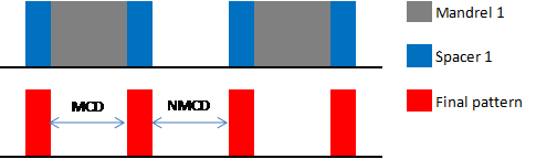
2.1. Line Cut on Positive Tone Self-aligned Patterning
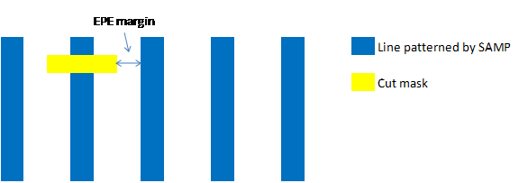
Final pattern follows the spacer pattern in positive tone self-aligned patterning, so line cut can be performed either on spacer /HM underneath spacer (cut first) or final pattern (cut last). Benefit of cut last is good CD uniformity due to better etch loading effect since there is only dense structure during final pattern etch, ISO or semi-ISO structures only formed after line cut. While etch process for HM cut at cut first is relatively easier since the HM height is much lower than final pattern, also we can play with HM CD at cut first for higher EPE margin. As show in Figure 5, EPE margin refers to distance between cut mask edge and nearest line edge which should not be cut. EPE margin equals line space/2. EPE margin increased if line CD reduced at a fix pitch.


Figure 5.   EPE margin.
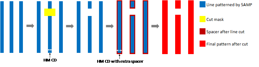
2.1.1. One idea as Figure 6 below is to start with thinner spacer thickness so that smaller HM CD after SAMP, then do the cut first on this smaller HM CD for higher EPE margin. One extra spacer deposited on HM after line cut to target the final CD per design. EPE margin improvement equals (HM CD with extra spacer - HM CD)/2 [[9]].


Figure 6.   
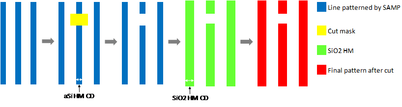
Line cut EPE margin improved with smaller HM CD.
2.1.2. Another idea as shown in Figure 7 is similar with idea above which is also start with thinner spacer thickness and cut first for higher EPE margin. Since the HM in this case is made with amorphous silicon, oxidization is applied on the HM to fully or partially convert amorphous silicon to silicon dioxide, 2.17 unit thickness of oxide will grow for every unit thickness of silicon consumed. Engineering work required for the oxidization process condition to meet the CD target for final HM etch [[10]].


Figure 7.   Line cut EPE margin improved with smaller aSi HM CD before oxidization.
2.2. Line Cut on Negative Tone Self-aligned Patterning
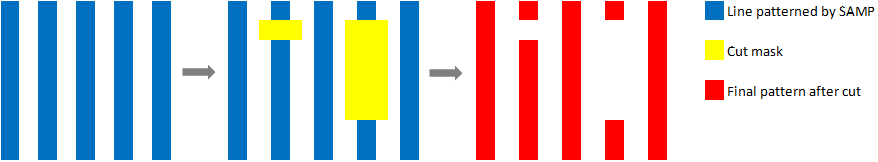
Final pattern is defined by space in between self-aligned spacers in negative tone self-aligned patterning. So, there is two way to do line cut: one way is to cut the mandrel which is called mandrel cut; the other way is to block the space in between spacers during final pattern etch which is called non-mandrel cut.
Typical non-mandrel cut as Figure 8 is to fill the space in between spacers with a different material, then remove the fill material at area no need line cut so that non-mandrel line cut by the block HM of the fill material [[11] ].


Figure 8.   Typical non-mandrel cut on negative tone self-aligned patterning.
Compare to non-mandrel cut, mandrel cut is more complicated since mandrel material at line cut region need to be replaced with a different material so that which works as HM during final pattern etch. Next I will focus on ideas to make the mandrel cut.
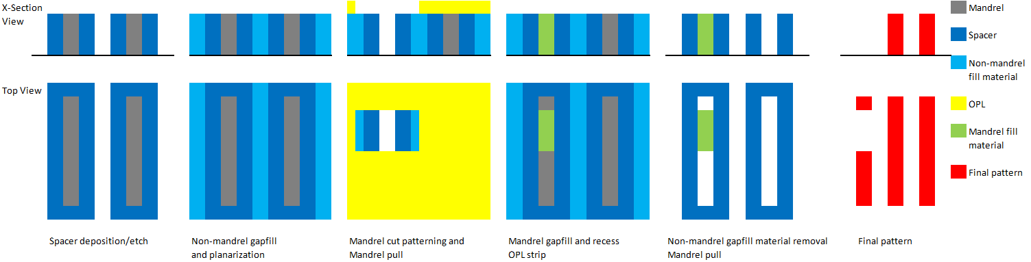
2.2.1. Mandrel Cut after Spacer Deposition
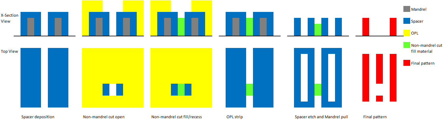
 [[12], [13]]
After spacer deposition, a typical mandrel cut as Figure 9 is to fill the space in between spacers with a different material after spacer etch to expose mandrel followed by planarization, then remove mandrel at mandrel cut area and filled with other material followed by recess which will work as HM for mandrel cut.


Figure 9.   
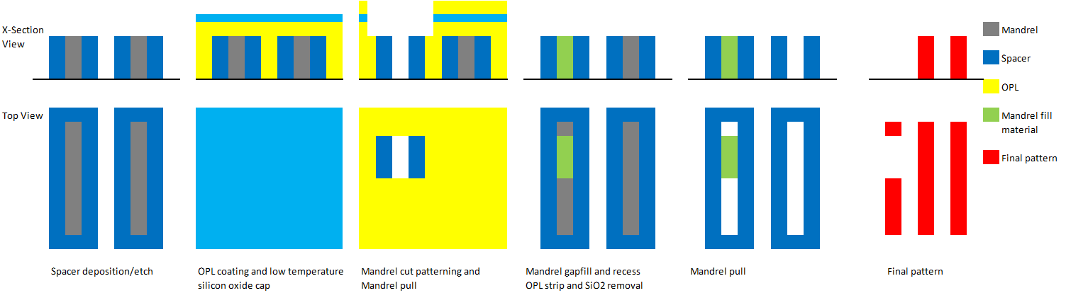
Mandrel cut after spacer deposition.
Optimized version of above idea as Figure 10 is to fill the space in between spacer with spin on carbon based optical planarization layer (OPL) material followed by a low temperature silicon oxide capping so that can do pattern on top of it without affecting the OPL underneath. The following steps for mandrel cut are similar as above idea.


Figure 10.   Optimized version of mandrel cut after spacer deposition.
2.2.2.   
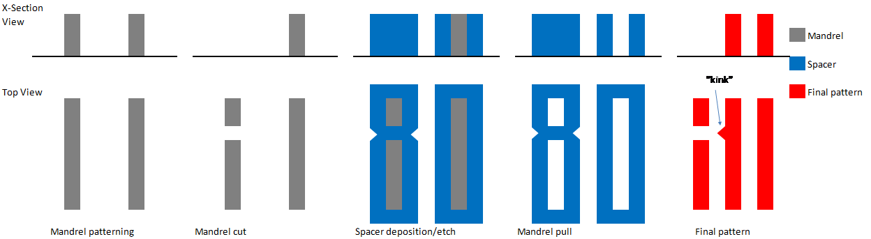
Mandrel Cut before Spacer Deposition [[11]]
Instead of cut mandrel after spacer deposition which require extra fill process to fill the mandrel cut region, this idea as Figure 11 is to cut mandrel before spacer deposition and make sure the cut width is less than 2x of spacer thickness so that the mandrel cut will be filled or pinched off by spacer deposition afterwards which will works as HM for mandrel cut. Both advantage and disadvantage of this idea are quite straightforward that it can enable mandrel cut without extra fill process while the cut CD is limited to less than 2x of spacer thickness. And higher line resistance observed for Cu interconnects patterned with this method due to the “kinks” formed by spacer pinch off.


Figure 11.   Mandrel cut before spacer deposition.
2.2.3.   
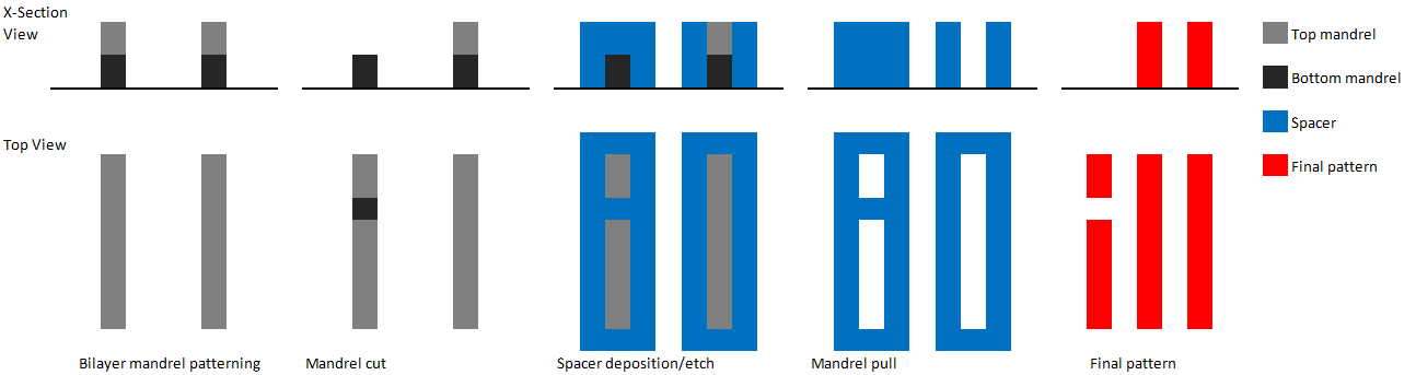
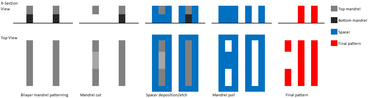
Bilayer Mandrel for Mandrel Cut [[14]]
One idea as Figure 12 to improve the Cu line resistance caused by the “kinks” is to change the mandrel material from single layer to bilayer with etch selective for the two materials in the bilayer. So the mandrel cut before spacer deposition is only cut the top layer of mandrel so that even the spacer pinch off at the top layer mandrel cut region, the bottom layer mandrel will still “straighten up” the spacer at bottom so that no “kinks” after final etch.


Figure 12.   Top mandrel cut before spacer deposition.
While the cut CD limitation <2x spacer thickness still not improved with above method, an optimized version of bilayer mandrel idea proposed as below Figure 13 to enable variable space mandrel cut before spacer deposition. The main difference to above bilayer mandrel cut is to cut the bottom layer mandrel with top layer mandrel intact before spacer deposition so that the mandrel cut will be filled with spacer material during spacer deposition which will works as HM for mandrel cut.


Figure 13.   Bottom mandrel cut before spacer deposition.
2.2.4.   
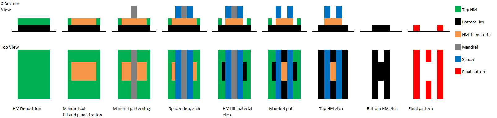
Mandrel Cut before Mandrel Deposition [[15]]
Another idea to cut mandrel as Figure 14 is to cut the HM underneath mandrel and filled with different material with etch selectivity to mandrel and HM which will works as HM for mandrel cut during final pattern etch.


Figure 14.   Mandrel cut before mandrel deposition.
2.3.   
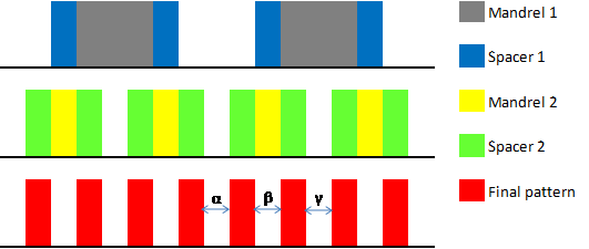
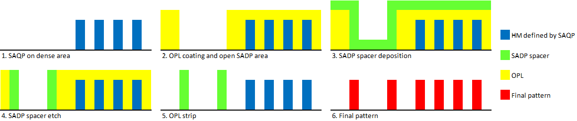
SADP and SAQP on Same Chip [[16]]
Pattern density is different on different function area of same chip. For example, logic area has higher pattern density than SRAM area which requires SAQP for patterning so that more lines need to be cut at SRAM area. Instead of pattern the lines with SAQP and cut it afterwards, idea below as Figure 15 enabled SADP at low density area such as SRAM and SAQP at high density area such as logic so that overall less line cut required.


Figure 15.   SADP and SAQP on same chip.
3.   Conclusion
In this paper we discussed some recent novel ideas of line cut on both positive and negative tone self-aligned patterning. Line cut with 193nm immersion lithography will face more and more challenges as the scaling continues. I see the trend in future for line cut of SAMP will be self-aligned or with EUV lithography.
[1] G. E. Moore, "Cramming more components onto integrated circuits", Electronics, 38 (8), (1965).
[2] R. H. Dennard, F. H. Gaensslen, H-N Yu et al., "Design of ion-implanted MOSFET's with very small physical dimensions", Proceedings of the IEEE 87 (4), 668-678 (1999).
[3] C. Auth, A. Aliyarukunju, M. Asoro et al., “A 10nm High Performance and Low-Power CMOS Technology Featuring 3rd Generation FinFET Transistors, Self-Aligned Quad Patterning, Contact over Active Gate and Cobalt Local Interconnects”, IEDM, (2017).
[4] R. Xie, P. Montanini, K. Akarvardar et al., “A 7nm FinFET Technology Featuring EUV Patterning and Dual Strained High Mobility Channels”, IEDM, (2016).
[5] J. Hwang, J. Seo, Y. Lee et al., “A Middle-1X nm NAND Flash Memory Cell (M1X-NAND) with Highly Manufacturable Integration Technologies”, IEDM, (2011).
[6] P. Xu, Y. Chen, Y. Chen et al., “Sidewall spacer quadruple patterning for 15nm half-pitch”, Proc. of SPIE, 7973, (2011)
[7] T. Kagalwala, A. Vaid, S. Mahendrakar et al., “Scatterometry-based metrology for SAQP pitch walking using virtual reference”, Proc. of SPIE, 9778, (2016)
[8] E. Liu, A. Ko, R. Farrell et al., “Multi-color approach on self-aligned multiple patterning for single line cut application”, Proc. of SPIE, 10584, (2018)
[9] G. Derderian, “Fin cutting process for manufacturing FinFET semiconductor devices”, US Patent 9,754,792, (2017)
[10] J. Shu, G. Derderian, J. Liu, “Methods for forming fins”, US Patent 10,276,374, (2019)
[11] J. E. Stephens, G. Bouche, “Method of patterning pillars to form variable continuity cuts in interconnect lines of an integrated circuit”, US Patent 9,852,986, (2017)
[12] J. Shu, B. Kim, J. Liu, “Variable space mandrel cut for self aligned double patterning”, US Patent 10,199,265, (2019)
[13] J. Shu, J. Liu, R. Chen, “Multiple patterning with variable space mandrel cuts”, US Patent Application 20190067010 (2019)
[14] X. Wang, J. Shu, B. O’Brien et al., “Self-aligned multiple patterning processes using bi-layer mandrels and cuts formed with block masks”, US Patent 10,192,780, (2019)
[15] J. Shu, Q. Fang, D. W. Fisher et al., “Self-aligned lithographic patterning with variable spacings”, US Patent 9,711,447, (2017)
[16] J. Shu, D. Jaeger, G. Derderian et al., “Devices and methods of forming SADP on SRAM and SAQP on logic”, US Patent 9,761,452, (2017)
Article and author information
Jeff Shu
jeff.shu@globalfoundries.com
Publication records
Published: Sept. 25, 2019 (Versions1
References
Journal of Microelectronic Manufacturing