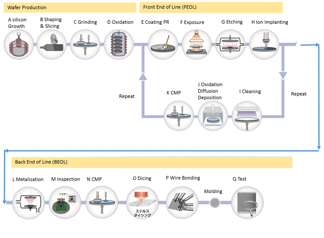
Our everyday electrical and electronic devices like PCs, iPhones, iPads contain numerous semiconductor devices or ICs. Most semiconductor devices will experience three periods: wafer preparation (production of wafer), front end of line and back end of line, as shown in Figure 2.
Figure 2.
Semiconductor Device Manufacturing Process Flow. During wafer preparation, sands in the environment will go through several steps (mainly like silicon growth, shaping & slicing, grinding and oxidation) and finally become silicon wafers. In silicon growth (A), silica (SiO2), pure sand will be firstly transformed to metallurgical-grade silicon (MSG) and finally to semiconductor-grade silicon (SGS) according to several complex chemical reactions which are mainly generated in mono-crystal furnaces. After horizontal spinning and vertical pulling of mono-crystal furnaces, silicon ingots are prepared. But it is difficult to make all silicon ingots grow quite vertically and keep the same diameter. In this term, low resolution, large area, high speed CCD image sensors or cameras are often used to measure the diameter. If the shape is not good enough, shaping must be done before slicing (B).
In order to achieve a smooth wafer surface with a high degree of flatness and obtain desired thickness which is the result of combination of physical and chemical reactions, grinding (C) is an indispensable step. Low resolution, large area CCD image sensors or cameras are useful in this time to measure the flatness. From Table 1, the thickness of 4'' Si wafer is about 525 μm while 18'' Si wafer would be about 925μm, so the useful thin film thickness measurement system like C11011 should have a detection range wider than that. During grinding, there will be some electrostatic charges on the surface of Si wafer due to the contact between Si wafer and a certain material (like metal, slurry, chemical materials or other material). According to ITRS Technology Roadmap for Semiconductors Electrostatics 2005, for 50 nm node and beyond, maximum allowable static charge on device is 0.25 nC (25V). Actually, electrostatic charges easily generates during the whole semiconductor manufacturing process (including FEOL and BEOL) flow due to the wafer transport, chucking / de-chucking, process itself and other factors
[8]. Hamamatsu offers two kinds of electrostatic charge removers. One is for vacuum use (VUV Ionizer), another is for non-vacuum use (PhotoIonizer). They both use special light sources to ionize the charged particle on the surface of the Si wafer and then remove it by electrostatic attraction.
Thereafter, process engineers will grow a thin oxidation layer or epitaxy layer above the Si wafer due to process needs and in this case we again need to use thin film thickness measurement system to check whether the thickness is qualified or not. In semiconductor manufacturing, a blank wafer (or unpatterned wafer) is prepared to feature a certain process like thermal oxidation. If there are some defects on bare wafers, it will largely influence the featuring of the process and eventually influence the yield. So the inspection of bare wafer is quite important. In unpatterned wafer defect inspection application, Hamamatsu provide an advanced light source, laser driven light source (LDLS) which has wide spectral sensitivity (170 ~ 2100 nm), long lifetime (>9000 h), high stability and high brightness so that LDLS is quite suitable. In detectors parts, Hamamatsu provides various types of CCD/CMOS/NMOS image sensors (line, area, TDI and InGaAs) and CMOS/CCD cameras (line, area, TDI and InGaAs) for different design ideas. Photomultiplier tubes (PMT), due to its extremely high gains (106~107), can be another choice to detect faint scattering light.
Table 1.
Diameters and Thicknesses of Si wafers | Diameters (mm) | Diameters (inches) | Thickness (μm) |
450
300
200
150
100 | 18
12
8
6
4 | 925
775
725
675
525 |
Front end of line (FEOL) refers to every processes until metallization (the deposition of metal interconnect layers)
[9] and outcomes the patterns of the individual devices like transistors, capacitors, resistors and etc. FEOL is the essence of IC fabrication and largely influence the performance of ICs. The main processes in FEOL are lithography (pre-curing, photoresist (E), exposure (F), post-curing, developing and etc.), etching (G), ion implanting (H), cleaning (I), oxidation/diffusion/deposition (J), chemical mechanical polishing (CMP) (K).
After coating photoresist (E), etching (G), deposition/oxidation (J) and CMP (K), thin film thickness measurement systems are needed to check whether the film thickness is qualified. UV camera, mini-spectrometer and plasma process monitor are able to measure the spectrum and determine the end of point in exposure (F). S10121/S10122/S10123/S10124 series image sensor have high UV sensitivity, high linearity which can monitor wavelength and measure alignment. 200 w/350 w Hg-Xe light sources may worth a try for low cost lithography machine.
Like lithography machine, in process equipments of etching (G), deposition (J) and ion implanting (H), plasma process monitor or mini-spectrometer are integrated to measure the spectrum and detect the end of point. When wafer goes through lithography, its surface will print the copy of photomask's pattern and then wafer is no longer bare (blank or unpatterned) wafer but patterned wafer. Comparing with unpatterned wafer defect inspection, patterned wafer defect inspection needs find the fine deviation between process results and process designs in short time which requires high power, long lifetime, shorter wavelength and stable light sources and high sensitivity, high response speed and wavelength-matching photodetectors. Hamamatsu strongly recommend LDLS (EQ-99 series, 170 ~2100 nm) or EUV light sources (EQ-10 series, 13.5 nm) plus customized TDI CCD image sensor/camera as the emitter-receivers solutions. EQ-10 series EUV light sources based on Z pinch electrodeless technology are quite suitable for EUV metrology, inspection and research applications. Those light sources have high power, stable, long life time, broadband spectrum including UV or EUV to IR wavelength and other features. TDI CCDs are suitable for imaging moving objects in low light level because it keeps the transferring integrated signal charges synchronized with object’s movement
[10]. But before it works, we should make sure that line rate multiply pixel size equals motion speed of object. In addition, for general optical inspection including imaging, flash Xe lamps, Xe lamps, Hg-Xe lamps, Deuterium lamps as light sources, line image sensors / cameras (line, area, TDI and InGaAs) and mini-spectrometers are also recommended according to specific scenes.
Back end of line (BEOL) is like wearing clothes for a human body. It starts from metallization to final test, including metallization (L), inspection (M), CMP (N), slicing (O), wire bonding (P), molding and test. CMP (N) is quite the same as CMP (K). Slicing is the procedure to cut the dice on a wafer into chips. Hamamatsu’s stealth dicing machine is different from traditional blade dicing and laser ablation dicing. It is internal absorption laser process and is neither grinding cutting or surface absorption laser process so that SDE is able to enhance yield, generate no debris and save water.
The outcomes of BEOL are IC chips but unfortunately not all IC chips can function well. IC chips may fail due to various reasons like scratches, defects and etc. Hamamatsu provides manufacturers of semiconductor devices and assembled products with excellent failure analysis (FA) systems including functions of IR-Obirch Analysis, dynamic analysis, emission analysis, thermal analysis, and backside analysis in IC designing, FEOL and BEOL. Using FA systems, engineers can easily locate defects and compare them with designing/manufacturing documents so that they can find what is wrong in designing or manufacturing.
In BEOL, voids, protrusions, copper hillocks, remaining metal, under-polish of copper of barrier, over-polish, scratches, embedded contamination, chatter marks, dielectric rip-outs, peeling, corrosion, residual slurry and so on are common defects which will influence the function of IC chips. Effective optical inspection must be implemented in order to enhance yield. Like in FEOL, LDLS, Xe lamps, flash Xe lamps and IR LEDs are good choices for light sources while various types of image sensors/cameras, PMTs, photodiode, APD, MPPC are common choices for light receivers.
3. Features of Some Light Sources and Photodetectors
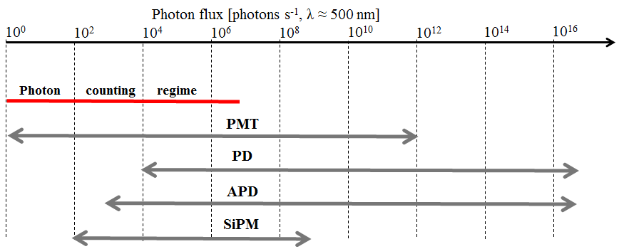
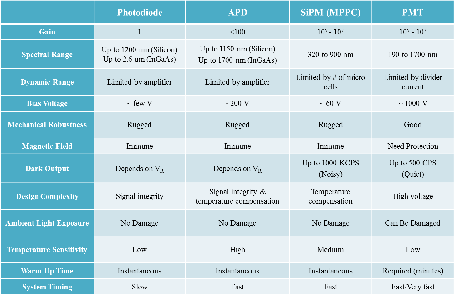
In section 2, light sources and photodetectors which can be used in semiconductor devices fabrication process flow are listed. Photodiodes, APDs, SiPMs (MPPCs) and PMTs are common point sensors and can be arrayed to detect larger area. From Figure 3, PMTs have wider light dynamic ranges than PDs, APDs and SiPMs, since photon counting to 1012 Photon flux and PMTs usually have very low dark outputs so that PMTs are well suitable for low light detection. But PMTs need special magnetic shielding because magnetic field will influence the electron trajectory. PMTs have high gain so that PMTs may become damaged when exposed to ambient light. Generally speaking, due to wide spectrum, high gain, high dynamic range and low temperature sensitivity and low dark output, PMTs are good point sensors to be used in process equipments and inspection equipments.
Figure 3.
Incident light levels of PD, APD, SiPM and PMT. Figure 4.
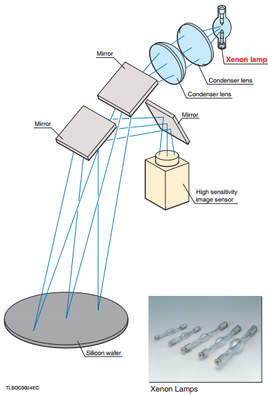
Comparisons between PD, APD, SiPM and PMT [11]. When selecting an appropriate light source, some features like wavelength, output power, stability, lifetime, noise and price are key factors. From Table 2, LDLS has long spectral response from DUV to IR and has higher output power, better stability, longer lifetime and lower noise. The price of LDLS is higher than D2 (Deuterium) lamps, Xe lamps and LEDs but if you consider it overall, you will find LDLS is quite cost effective. Figure 5 is a traditional structure of the detection system of wafer inspection equipments with a Xe lamp. After entering 10 nm era, the brightness of Xe or Flash Xe lamps may hardly meet the requirement for precise defect inspection including wafer inspection and photomask inspection. In this time, LDLS and EQ-10 series are definitely the assets. Considering about the price and volume, Xe lamps, flash Xe lamps and LEDs still have their own places.
Table 2.
Comparisons among Light Sources | Attributes | D2 | Xe | LED | LDLS |
Wavelength
Brightness
Stability
Lifetime
Noise | UV
Medium
Low
Short
Low | UV - IR
Medium
Low
Short
High | Narrow
Low
Medium
Long
High | DUV – IR
High
High
Long
Low |
| Price | Medium | Medium | Cheap | High |
Figure 5.
A traditional structure of the detection system of wafer inspection equipments.